Low voltage high speed TTL and Not gate circuit and its method for improving operation speed
A non-gate circuit and operating speed technology, which is applied in the direction of improving switching speed and logic circuits with logic functions, etc., can solve the problems of large saturation storage time and power consumption, and achieve the effect of avoiding the effect of desaturation
- Summary
- Abstract
- Description
- Claims
- Application Information
AI Technical Summary
Problems solved by technology
Method used
Image
Examples
Embodiment Construction
[0045] Symbol in the figure: V x1 = V(x1), V x2 = V(x2), V y = V(y), V b1 = V(b1), V c1 = V(c1), V b2 = V(b2), I b2 =IB(Q2),I e3 = IE(Q3), I e4 = IE(Q4), I c4 = IC(Q4), I e11 = IE(Q11), I e12 = IE(Q12), I Rb2 = I(Rb2), I Vc =I(VC ).
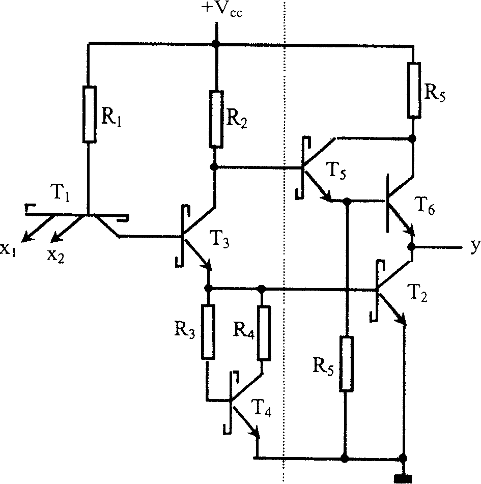
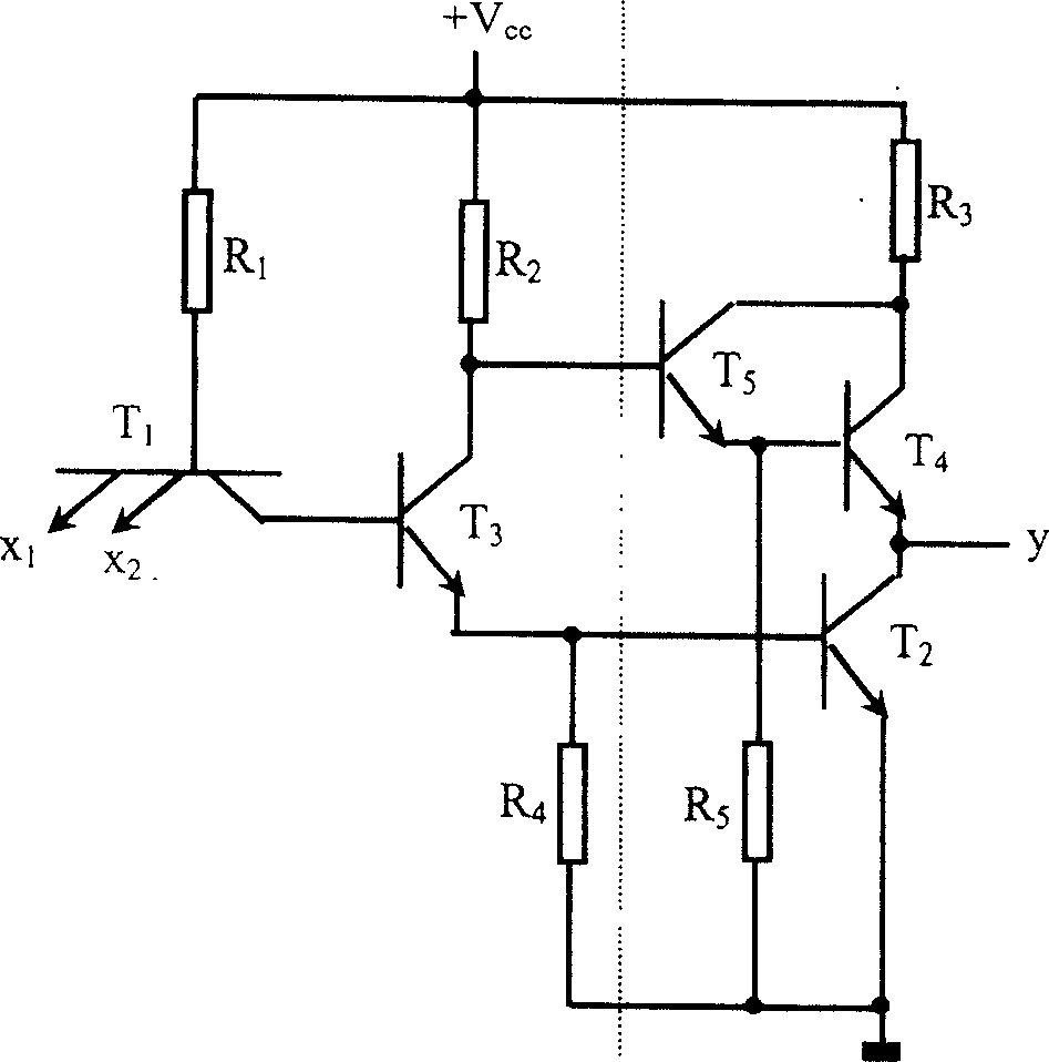
[0046] The TTL NAND gate circuit of the present invention includes two parts, a logic stage and an output stage. The input to the logic stage is x 1 and x 2 , the logic stage output is Q 2 base of the tube b 2 , enter x 1 、x 2 and output b 2 There is an 'and' relationship between them, that is, b 2 =x 1 x 2 . The output stage is an inverter, the output stage input b 2 There is a non-relationship between output y. First of all, no specific regulations are proposed for all transistors in the logic level, including the desaturation time t s Size, as long as the logic level input and output can achieve the purpose of fast following, forward driving and reverse extraction, and then reverse the requirements for each of the tri...
PUM
 Abstract
Description
Claims
Application Information
 - R&D Engineer
- R&D Manager
- IP Professional
- Industry Leading Data Capabilities
- Powerful AI technology
- Patent DNA Extraction
Browse by: Latest US Patents, China's latest patents, Technical Efficacy Thesaurus, Application Domain, Technology Topic, Popular Technical Reports.
© 2024 PatSnap. All rights reserved.Legal|Privacy policy|Modern Slavery Act Transparency Statement|Sitemap|About US| Contact US: help@patsnap.com


