Stacked layered type semiconductor memory device

A storage device and semiconductor technology, applied in the fields of semiconductor devices, semiconductor/solid-state device components, information storage, etc., can solve the problems of low chip yield and excessive chip economy.

Active Publication Date: 2005-07-27
SEIKO EPSON CORP
View PDF1 Cites 10 Cited by
  • Summary
  • Abstract
  • Description
  • Claims
  • Application Information

AI Technical Summary

Problems solved by technology

At this time, in order to manufacture different chips, not only different metal masks are required, bu

Method used


Image

  • Stacked layered type semiconductor memory device
  • Stacked layered type semiconductor memory device
  • Stacked layered type semiconductor memory device

Examples


Embodiment Construction

[0021] Hereinafter, embodiments of the present invention will be described with reference to the drawings.

[0022] 1. Lamination of semiconductor memory devices

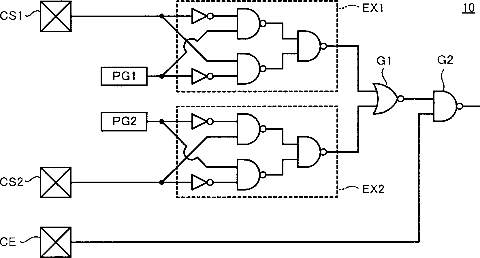
[0023] figure 1 It is a schematic perspective view of an example of three-dimensional mounting of a stacked semiconductor memory device according to an embodiment of the present invention. In this semiconductor memory device, four identical memory cell array chips C1-C4 are laminated to obtain a memory capacity that is four times the average area. These chips C1 to C4 correspond to the chip layer of the present invention.

[0024] In the chips C1 to C4, a plurality of chip select pads CS1, CS2 and one chip enable pad CE are respectively formed. Also, for simplicity in figure 1 It is not recorded in , but other pads necessary for storage operations, such as address or I / O, control pads, etc., are also formed. The number of chip select pads can be taken arbitrarily according to the number of stacked chips. In th...


PUM


Abstract

To provide laminated type semiconductor memory devices that can improve the yield of chips without complicating wirings and components. There are provided a plurality of laminated semiconductor chip layers, and chip selection pads provided on each of the chip layers, which are mutually connected across the chip layers, respectively, such that a chip selection signal for selecting each of the chip layers is commonly inputted in each of the chip layers. Each of the chip layers is equipped with program circuits each of which is capable of programming an output signal, and a chip selection judging circuit that judges a chip selection based on the chip selection signal and an output signal of the program circuit. As a result, address information can be set afterwards by the program circuit, such that one kind of chips may suffice in the chip manufacturing stage. Because the chip selection signal is inputted in the common chip selection pads, independent wirings for the respective chips are not required.

Description

technical field [0001] The present invention relates to a semiconductor storage device such as a ferroelectric storage device, and particularly relates to a technique for stacking a plurality of semiconductor chip layers and performing three-dimensional mounting according to a packaging technology so that the storage capacity of the area is several times that of a stacked chip, The individual chip layers can be chosen arbitrarily. Background technique [0002] In order to increase the density of semiconductor integrated circuits, a plurality of semiconductor chip layers are generally stacked. In order to drive the stacked semiconductor chips, it is necessary to have a structure for selecting which layer is activated. For example, JP-A-5-63138 discloses a structure in which semiconductor chips stacked on a carrier substrate are connected to one end of wires, and the other ends of the wires are connected to conductive pins provided on the carrier substrate. [0003] However,...

Claims


Application Information

Patent Timeline
IPC IPC(8): G11C11/22G11C7/00G11C8/12H01L23/12H01L25/065H01L25/07H01L25/18H01L27/10H01L27/105
CPCG11C5/02H01L2924/0002H01L2225/06513H01L2225/06541G11C8/12H01L25/0657G11C11/22H01L27/105H01L27/11509H01L2225/06527H10B53/40H01L2924/00H01L23/12H01L25/065
Inventor 小出泰纪
Owner SEIKO EPSON CORP
Why Eureka
Try Eureka