Semiconductor device
A semiconductor and conductivity technology, applied in semiconductor devices, semiconductor/solid-state device manufacturing, transistors, etc., and can solve problems such as insufficient variation
- Summary
- Abstract
- Description
- Claims
- Application Information
AI Technical Summary
Problems solved by technology
Method used
Image

Examples
no. 1 approach
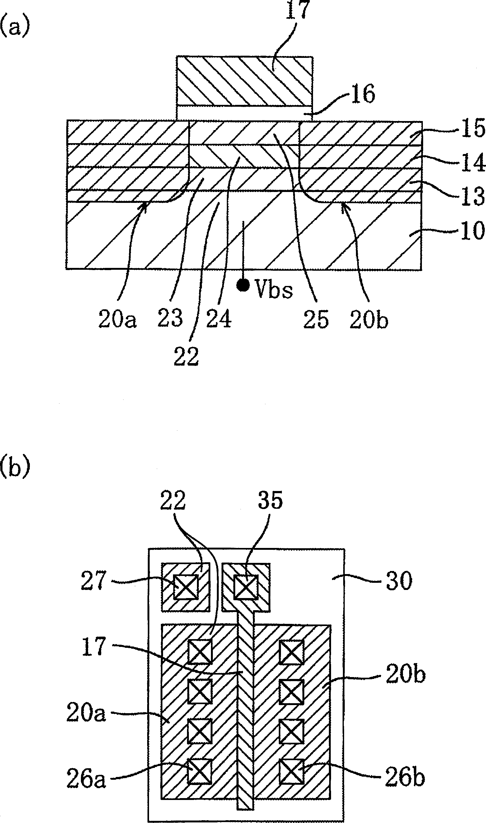
[0049] figure 1 (a) and (b) are cross-sectional and plan views of a heterojunction p-channel VTMIS transistor (hereinafter referred to as pHVTMISFET) using the SiGe layer of the first embodiment of the present invention as a channel.
[0050] Such as figure 1 (a) and (b) show that the pHVTMISFET of this embodiment includes a p-type Si substrate 10, a Si buffer layer 13 with a thickness of about 10 nm epitaxially grown on the Si substrate 10 by UHV-CVD, and a Si buffer layer 13 on the Si buffer layer 13. A SiGe film 14 with a thickness of about 15 nm (30% Ge occupancy) epitaxially grown by UHV-CVD and a Si gap layer 15 with a thickness of about 5 nm epitaxially grown on the SiGe film 14 by UHV-CVD.
[0051] Further, the pHVTMISFET includes a gate insulating film 16 formed of a silicon oxide film with a thickness of about 6 nm provided on the Si gap layer 15 and a gate electrode 17 provided on the gate insulating film 16 . The gate electrode 17 is made of polycrystalline silic...
no. 2 approach
[0099] In this embodiment mode, an example in which the present invention is applied to a complementary HVTMIS device (cHVTMIS device) having a SiGe channel will be described.
[0100] Figure 13 (a), (b), and (c) are diagrams showing the configuration of the cHVTMIS device of the present embodiment, Figure 13 (a) is a cross-sectional view showing the structure of the cHVTMIS device of this embodiment, Figure 13 (b) is an energy band diagram showing the band state of pHVTMISFET when a gate bias voltage is applied (during operation), Figure 13 (c) is an energy band diagram showing the band state of the nHVTMISFET when a gate bias is applied (during operation).
[0101] Such as Figure 13 As shown in (a), the cHVTMIS device of this embodiment has a p-type Si substrate 10, an embedded oxide film 11 formed by implanting oxygen ions into the Si substrate, etc., and a p-channel type oxide film 11 formed on the embedded oxide film 11. The semiconductor layer 30 for the HVTMISF...
no. 3 approach
[0110] In the above-mentioned first and second embodiments, although the channel region is made of SiGe, the channel region may be made of SiGeC having a C (carbon) occupancy of 0.01% to 2% (for example, about 1%). If a small amount of C is added to the SiGe channel region, the effect is further enhanced. Although SiGe crystals tend to have a strong tendency to cause undesired changes in the crystal structure due to ion implantation, by constituting the channel region with SiGeC, undesired changes in the crystal structure due to ion implantation can be suppressed.
[0111] Figure 14 (a), (b), and (c) are diagrams showing the configuration of the cHVTMIS device of the present embodiment, Figure 14 (a) is a cross-sectional view showing the structure of the cHVTMIS device of this embodiment, Figure 14 (b) is an energy band diagram showing the band state of the pHVTMISFET when a gate bias is applied (during operation), Figure 14 (c) is an energy band diagram showing the ban...
PUM
 Abstract
Description
Claims
Application Information
 - R&D
- Intellectual Property
- Life Sciences
- Materials
- Tech Scout
- Unparalleled Data Quality
- Higher Quality Content
- 60% Fewer Hallucinations
Browse by: Latest US Patents, China's latest patents, Technical Efficacy Thesaurus, Application Domain, Technology Topic, Popular Technical Reports.
© 2025 PatSnap. All rights reserved.Legal|Privacy policy|Modern Slavery Act Transparency Statement|Sitemap|About US| Contact US: help@patsnap.com