
Photosensitive thick-film paste materials for forming light-transmitting electromagnetic shields, light-transmitting electromagnetic shields formed using the same, and method of manufacture thereof

An electromagnetic shielding and thick film technology, applied in the application of optical/shielding coatings, magnetic field/electric field shielding, photosensitive materials for optomechanical equipment, etc., can solve the problem of unused, difficult to obtain metal area resolution, etc. question

Inactive Publication Date: 2005-05-25
EI DU PONT DE NEMOURS & CO
View PDF13 Cites 7 Cited by
  • Summary
  • Abstract
  • Description
  • Claims
  • Application Information

AI Technical Summary

Problems solved by technology

[0009] However, it is difficult to obtain resolution in the metal area that provides an appropriate aperture ratio by using a printing method that alone forms an electromagnetic shield.
Therefore, this method is not currently used

Method used


Image

  • Photosensitive thick-film paste materials for forming light-transmitting electromagnetic shields, light-transmitting electromagnetic shields formed using the same, and method of manufacture thereof
  • Photosensitive thick-film paste materials for forming light-transmitting electromagnetic shields, light-transmitting electromagnetic shields formed using the same, and method of manufacture thereof
  • Photosensitive thick-film paste materials for forming light-transmitting electromagnetic shields, light-transmitting electromagnetic shields formed using the same, and method of manufacture thereof

Examples


example

[0099] The total amount of all ingredients making up the composition is partially described in each example.

[0100] FODEL(R) silver paste manufactured by DuPont was used as a photosensitive thick-film conductive paste, FODEL(R) ruthenium oxide paste manufactured by DuPont was used as a photosensitive thick-film black paste, and soda-lime glass having a thickness of 2.5-3 mm was used as a glass substrate. For good visibility, the glass substrate must be of good quality, free from defects such as internal bubbles and surface scratches.

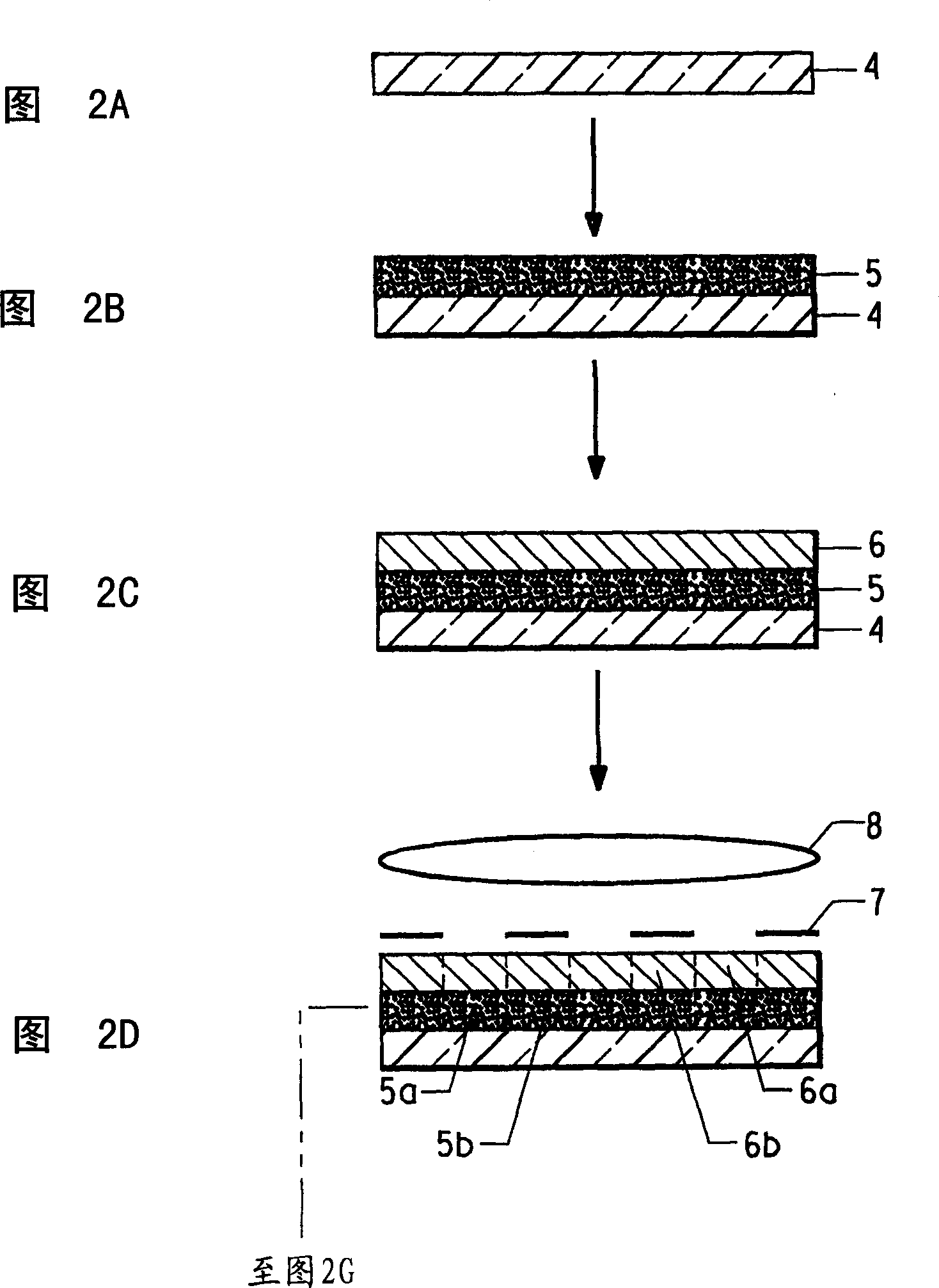
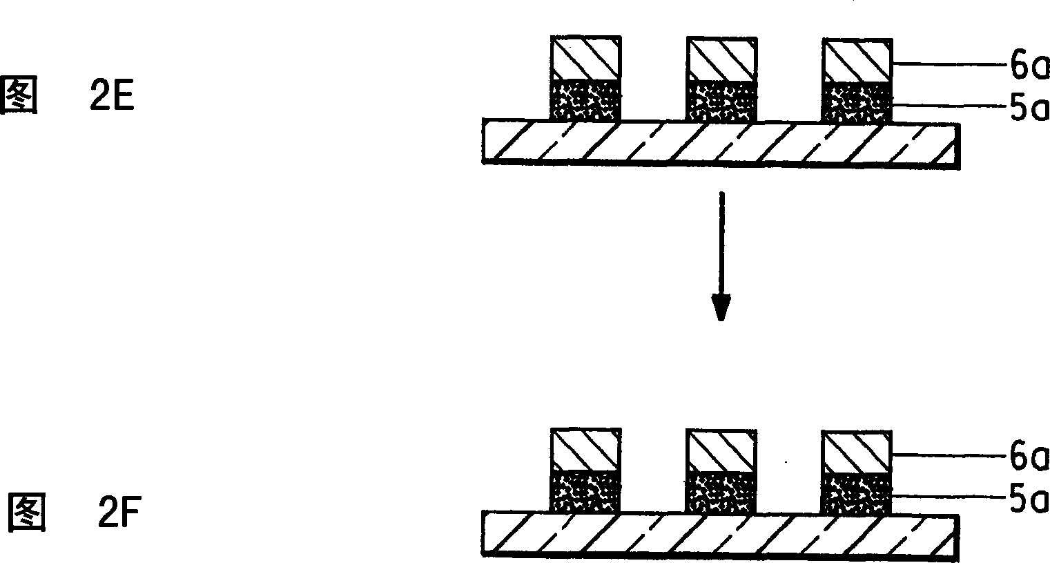
[0101] FODEL® ruthenium oxide paste (manufactured by DuPont) was used as a photosensitive thick film black paste, and the photosensitive thick film black paste was screen printed onto a 2x3 inch glass substrate (high yield point glass) by using a 380 mesh polyester screen. PD200, manufactured by Asahi Glass Co., Ltd.), and in a batch-type hot air drying furnace, dry with a peak temperature of 80 ° C and a total of 20 minutes of profile (profil...


PUM

PropertyMeasurementUnit
thicknessaaaaaaaaaa
sizeaaaaaaaaaa
softening pointaaaaaaaaaa

Abstract

The present invention relates to a light-transmitting electromagnetic shield having an electromagnetic shield that reduces the emission of electromagnetic waves when mounted in front of a display such as a plasma display panel (PDP), cathode ray tube (CRT) or electroluminescent (EL) display performance, with high visible light visibility, low reflectivity to ambient light, and excellent durability.

Description

field of invention [0001] The present invention relates to a light-transmitting electromagnetic shield which, when installed in front of a display such as a plasma display panel (PDP), cathode ray tube (CRT) or electroluminescent (EL) display, has reduced Electromagnetic shielding performance for electromagnetic wave emission, high visible light visibility, low reflectivity to external light, and excellent durability. Background of the invention [0002] The rising performance of plasma displays and other large screen displays has led to a growing interest in techniques for shielding electromagnetic radiation emitted by display devices. In particular, as the use of display devices such as home televisions grows, the proportion of displays worldwide that are required to comply with the US Federal Communications Commission (FCC) Class B standard is steadily increasing. At the same time, attention shifted from concern about electromagnetic wave interference (EMI) between machi...

Claims


Application Information

Patent Timeline
Patent Type & Authority Applications(China)
IPC IPC(8): H01B1/20B32B9/00B32B15/04C03C17/36C03C17/40C09D4/02G03F7/00G03F7/004G03F7/027G09F9/00H01J9/20H05K1/09H05K3/02H05K9/00
CPCC03C17/36C03C17/3607C03C17/3634C03C17/3644C03C17/3655C03C17/3676C03C17/40C03C2217/44C03C2217/475C03C2217/479C03C2217/485C03C2218/119G03F7/0007G03F7/0047H01J9/205H01J2211/446H01J2329/869H05K1/092H05K3/02H05K9/0096H01B1/20
Inventor J·科伊施卡瓦T·穆托M·楚基亚
Owner EI DU PONT DE NEMOURS & CO
Learn More