MOS switching grid boosting circuits
A MOS tube and circuit technology, applied in the field of new MOS switch gate booster circuit, can solve problems such as increasing cost
Inactive Publication Date: 2005-05-11
FUDAN UNIV
View PDF0 Cites 0 Cited by
- Summary
- Abstract
- Description
- Claims
- Application Information
AI Technical Summary
Problems solved by technology
[0019] The most direct way to increase the gate-source voltage is to increase the power supply voltage of the circuit, but from the perspective of low-voltage systems, the cost is increased because one more power supply circuit is required
Method used
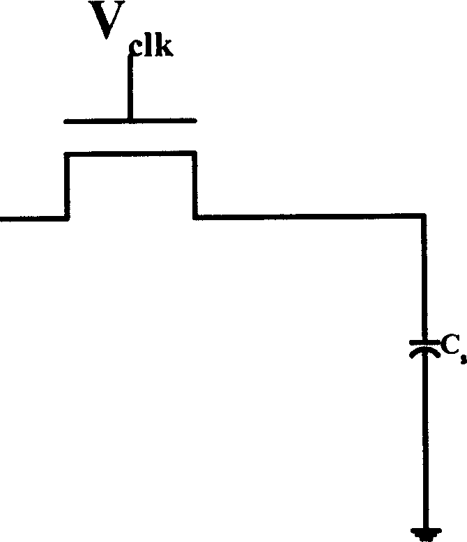
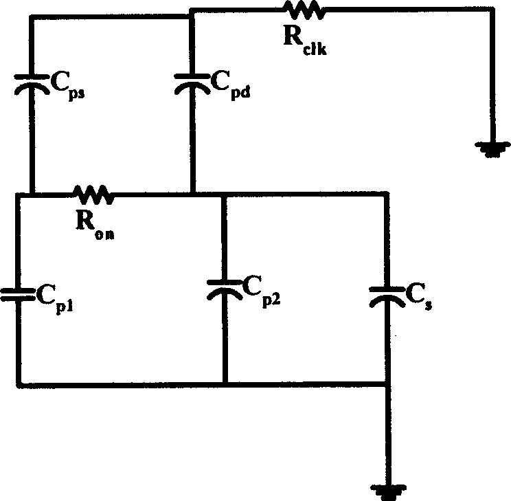
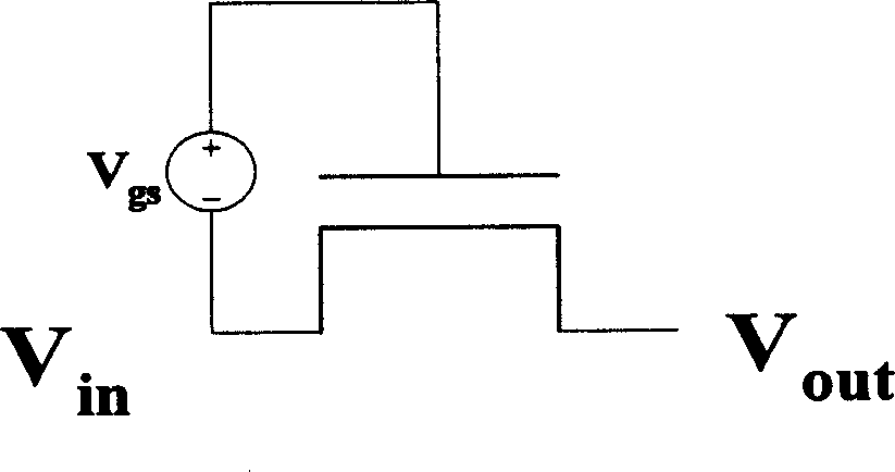
View moreImage
Smart ImageViewing Examples
Examples
Login to View More PUM
 Abstract
The invention can make the grating voltage of signal switch device not to relate to the input signals and keep on-resistance at constant, so that the loss of signals are greatly reduced. The substrate of NMOS switch circuit is always connected with lowest level of the circuit in this way the ordinary twin-hole CMOS technology can be easily implemented.
Description
technical field [0001] The invention belongs to the technical field of integrated circuits, and in particular relates to a novel MOS switch grid booster circuit. Background technique [0002] MOS type devices have excellent electrical characteristics as switches, so they are widely used in mixed signal circuits, such as switched capacitor circuits. But we know that the MOS type device is not an ideal switch. It has an on-resistance when it is turned on. The resistance value is related to the geometric size of the switching device and its gate voltage and threshold voltage. [0003] R on = 1 μC ox w l ( V gs - V t ) ...
Claims
Login to View More Application Information
Patent Timeline
 IPC IPC(8): H03K17/16H03K17/687
Inventor 张剑云张卫
Owner FUDAN UNIV
- R&D Engineer
- R&D Manager
- IP Professional
- Industry Leading Data Capabilities
- Powerful AI technology
- Patent DNA Extraction
Learn More Browse by: Latest US Patents, China's latest patents, Technical Efficacy Thesaurus, Application Domain, Technology Topic, Popular Technical Reports.
© 2024 PatSnap. All rights reserved.Legal|Privacy policy|Modern Slavery Act Transparency Statement|Sitemap|About US| Contact US: help@patsnap.com


