Ideal oxygen precipitating silicon wafers with nitrogen/carbon stabilized oxygen precipitate nucleation centers and process for making the same

An oxygen precipitation and stabilization technology, applied in semiconductor/solid-state device manufacturing, semiconductor devices, electrical components, etc., can solve problems such as loss of IG potential

Inactive Publication Date: 2005-04-13
MEMC ELECTONIC MATERIALS INC
View PDF4 Cites 8 Cited by
  • Summary
  • Abstract
  • Description
  • Claims
  • Application Information

AI Technical Summary

Problems solved by technology

As a result, all IG potential is lost

Method used


Image

  • Ideal oxygen precipitating silicon wafers with nitrogen/carbon stabilized oxygen precipitate nucleation centers and process for making the same
  • Ideal oxygen precipitating silicon wafers with nitrogen/carbon stabilized oxygen precipitate nucleation centers and process for making the same

Examples


Embodiment Construction

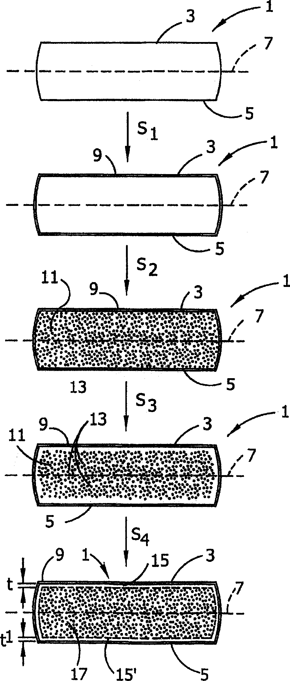
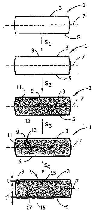
[0015] In accordance with the present invention there is disclosed an ideally deposited wafer which will form a clean zone of sufficient depth and a wafer body containing a sufficient density of oxygen deposits during essentially any electronic device fabrication process , the above oxygen precipitates are used for IG (intrinsic gettering) purposes. Advantageously, such ideally deposited wafers can be produced without problems using tools commonly used in the semiconductor silicon manufacturing industry. This method creates a "template" in the silicon that dictates or "prints" the way in which oxygen eventually precipitates. According to the invention, this template is stabilized such that it can undergo subsequent rapid thermal treatments (eg epitaxial deposition and / or oxygen implantation) without intervening thermal stabilization anneals.

[0016] A. Original material

[0017] The starting material for the desired deposited wafers of the present invention is a single crys...


PUM


Abstract

A silicon wafer having a controlled oxygen precipitation property so as to result in a clean zone extending inwardly from the front surface and oxygen deposits in the body of the wafer sufficient for intrinsic purpose of suction. Specifically, prior to the formation of oxygen precipitates, the wafer body includes dopant-stabilized oxygen precipitate nucleation centers. The dopant is selected from nitrogen and carbon and is present in a concentration sufficient to render the oxygen precipitate nucleation centers resistant to heat treatment such as an epitaxial deposition process while maintaining the ability to dissolve any growing nucleation centers.

Description

technical field [0001] The present invention generally relates to the preparation of substrates of semiconductor material, particularly silicon wafers, for use in the manufacture of electronic components. More specifically, the present invention relates to a method for processing silicon wafers that enables the wafers to develop a desired non-uniform depth profile of oxygen precipitates during the thermal treatment cycle of essentially any electronic device manufacturing process . Background technique [0002] Single crystal silicon, the starting material for most methods of manufacturing semiconductor electronic components, is usually produced by the so-called Czochralski method, in which a single crystal seed crystal is immersed in molten silicon and then grown by slow pulling. Because the molten silicon is contained in a quartz crucible, it is contaminated with various impurities, mainly oxygen. At the temperature of the silicon melt, oxygen enters the crystal lattice u...

Claims


Application Information

Patent Timeline
Patent Type & Authority Applications(China)
IPC IPC(8): H01L21/322
CPCH01L21/3225H01L21/3226H01L21/20H01L21/322
Inventor M·S·卢西亚诺J·L·利伯特R·J·菲利普斯M·库尔卡尼M·巴南S·J·布伦克霍斯特
Owner MEMC ELECTONIC MATERIALS INC
Why Eureka
Try Eureka