
Semiconductor light-emitting device and its manufacturing method

一种发光元件、制造方法的技术,应用在半导体激光器、半导体激光器装置、光波导半导体的结构等方向,能够解决难以熔融大口径基板表面、发光波长不稳定、难以形成多个形状一致凹部等问题

Inactive Publication Date: 2005-03-30
PANASONIC CORP
View PDF6 Cites 13 Cited by
  • Summary
  • Abstract
  • Description
  • Claims
  • Application Information

AI Technical Summary

Problems solved by technology

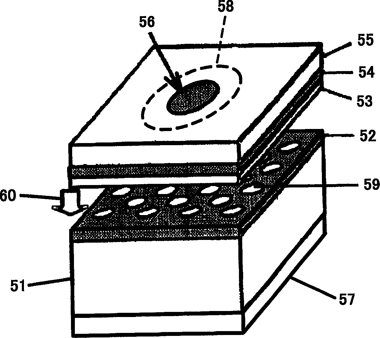
[0006] In this way, in the conventional semiconductor light emitting element, there is a problem that the threshold current is relatively large at 2A.
[0007] In addition, since the upper electrode 56 is a circular electrode, there is a problem that the polarization plane of light has various directions.
Furthermore, by making the shape of the concave portion 59 an ellipse to make the polarized planes uniform, it is difficult to form a plurality of elliptical concave portions 59 with the same shape.
[0008] In addition, even for light with the same polarization plane, there is a problem of unstable emission wavelength due to the existence of two stable emission modes
[0009] Furthermore, as described above, semiconductor light-emitting elements are produced by melting crystals, but there is a problem that it is difficult to melt the entire surface of a large-diameter substrate.

Method used


Image

  • Semiconductor light-emitting device and its manufacturing method
  • Semiconductor light-emitting device and its manufacturing method
  • Semiconductor light-emitting device and its manufacturing method

Examples


Embodiment approach 1

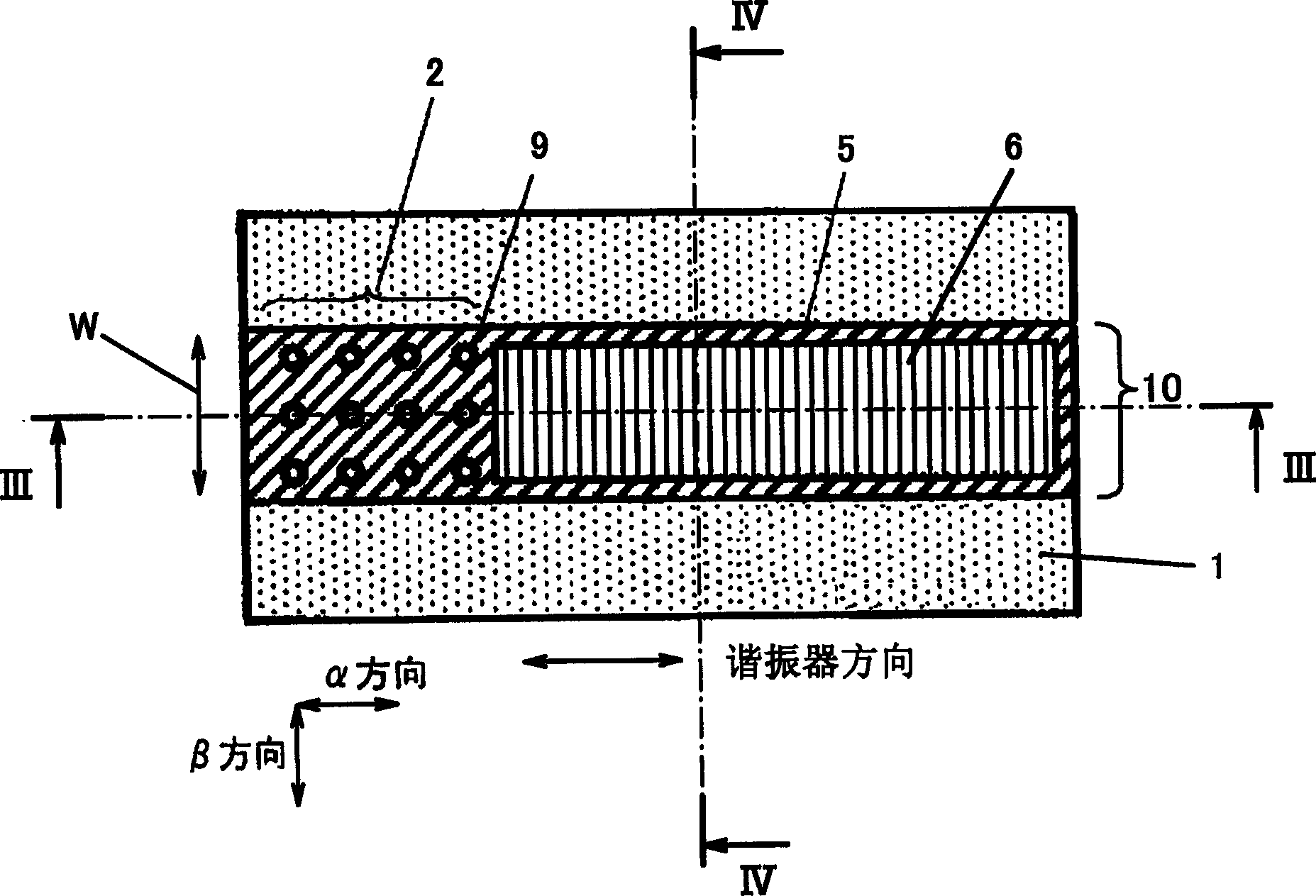
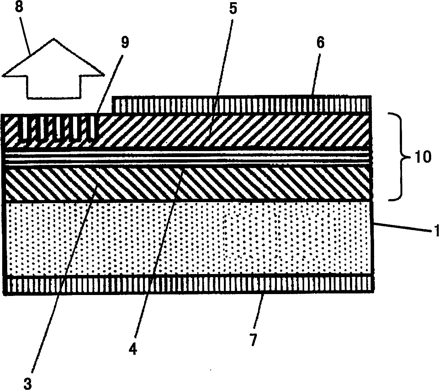
[0054] figure 2 It is a plan view showing the structure of the semiconductor light emitting element according to Embodiment 1 of the present invention. and image 3 Yes figure 2 The III-III line view, Figure 4 Yes figure 2 The IV-IV line view. In addition, the emission wavelength of the semiconductor light emitting element of this embodiment is 1.3 μm.

[0055] like Figure 2 to Figure 4 As shown, a stripe structure 10 is formed on an n-type InP substrate 1 . The stripe structure 10 is an n-type InP lower cladding layer 3 (thickness 100nm), an InGaAsP / InGaAsP quantum well active layer 4 (hereinafter referred to as the active layer 4 ), and a p-type InP upper cladding layer 5 (thickness 50nm). ) to form. Here, the active layer 4 is 5 pairs of In 0.9 Ga 0.1 As 0.2 P 0.8 Barrier layer (thickness 10nm, composition wavelength 1.1μm, lattice deformation 0%), In 0.9 Ga 0.1 As 0.5 P 0.5 A deformed quantum well structure composed of a well layer (thickness 4nm, quan...

Embodiment approach 2

[0081] In Embodiment 2, a semiconductor light-emitting element is shown in which there is a photonic crystal similar to Embodiment 1, but the period of the photonic crystal in the direction of the resonator is different from the period of the photonic crystal in the direction perpendicular to the direction of the resonator. .

[0082] Figure 8 It is a plan view showing the structure of the semiconductor light emitting element according to Embodiment 2 of the present invention. like Figure 8 As shown, the photonic crystal structure 2 is formed by arranging a plurality of recesses 9 in a rectangular lattice. Here, the period F1 of the recesses 9 in the resonator direction (interval between adjacent recesses 9 ) is longer than the period F2 of the recesses 9 in the direction perpendicular to the resonator direction. In addition, 13 in the figure represents a growth region when the p-type InP upper cladding layer is selectively grown as will be described later. In addition, ...

Embodiment approach 3

[0099] Embodiment 3 shows a semiconductor light emitting element in which leakage of naturally emitted light and induced emitted light in the direction of the resonator can be prevented by forming a reflective film that reflects light on the end surfaces of the stripe structure.

[0100] Figure 11 It is a figure showing the structure of the semiconductor light emitting element of Embodiment 3 of this invention, Figure 11 (a) is a plan view showing its structure, Figure 11 (b) is Figure 11 (a) A-A line view. like Figure 11 (a) and Figure 11 As shown in (b), an insulator multilayer thin film 11 made of alumina and titania is formed on both end surfaces of the stripe structure 10 . In addition, the other configurations of the semiconductor light-emitting element of this embodiment are the same as those of Embodiment 1, so the same reference numerals are assigned and descriptions thereof are omitted.

[0101] Hereinafter, a method of manufacturing the semiconductor lig...


PUM


Abstract

A semiconductor light emitting device of the present invention comprises a n-type InP substrate (1), and a stripe structure (10) formed in the stripe shape on the n-type InP substrate (1) and comprised of a n-type InP lower cladding layer (3), an active layer (4) having a resonator in a direction parallel to the n-type InP substrate (1), and a p-type InP upper cladding layer (5). The stripe structure (10) has a photonic crystal structure (2) with concave portions 9 arranged in rectangular lattice shape, and the direction in which the concave portions (9) of the photonic crystal structure (2) are arranged corresponds with a resonator direction. A stripe-shaped upper electrode (6) is formed on the stripe structure (10) to extend in the resonator direction. The semiconductor light emitting device of the present invention so structured is configured to radiate light in the direction perpendicular to the n-type InP substrate (1).

Description

technical field [0001] The present invention relates to a surface emission type semiconductor light emitting element using a photonic crystal grown on a substrate and a manufacturing method thereof. Background technique [0002] Conventional semiconductor light-emitting elements using photonic crystals are disclosed, for example, in (Japanese) Unexamined Patent Publication No. 11-330619, Japanese Unexamined Publication No. 2001-308457, and Japanese Unexamined Publication No. 2001-9800 (US Patent Publication No. 2002 / 0109134 No. Specification), JP-A-63-205984 (US Patent No. 4847844 Specification), JP-A-2002-062554, etc. [0003] In addition, similarly, it is also disclosed in 'Imada: Appl. Phys. Lett. 75 (1999) 316'. figure 1 It is a perspective view showing the structure of a conventional semiconductor light-emitting element using the photonic crystal disclosed in this "Imada". like figure 1 As shown, on an n-type InP substrate 51, an n-type InP photonic crystal layer 52,...

Claims


Application Information

Patent Timeline
Patent Type & Authority Applications(China)
IPC IPC(8): H01S5/028H01S5/10H01S5/12H01S5/18H01S5/187H01S5/22H01S5/40H01S5/42
CPCH01S5/028H01S5/105H01S5/2201H01S5/187H01S5/42H01S5/124H01S5/11
Inventor 大塚信之吉井重雄横川俊哉
Owner PANASONIC CORP
Learn More