
Memory control chip and data memory control method

A storage control and data access technology, applied in the design of storage control chips and in the field of data storage control, can solve the problems of occupying the working time of the processor, reducing the efficiency of the processor, affecting the flexibility of operation, etc. The effect of high speed and low error rate

Inactive Publication Date: 2005-02-09
NETAK TECH KO LTD
View PDF0 Cites 34 Cited by
  • Summary
  • Abstract
  • Description
  • Claims
  • Application Information

AI Technical Summary

Problems solved by technology

However, today's control chips with data checking and correctness guarantee functions cannot check the correctness of the data in real time during the data transmission process, but only check whether the transmitted data is correct after a section of data is transmitted. The correctness and integrity of the transmitted data cannot be guaranteed in real time; moreover, because the inspection and correction are performed after a period of data transmission, the working time of the processor is occupied and the efficiency of the processor is reduced
In addition, the DMA method of most storage control chips only provides one type of DMA transfer, such as from the first memory to the second memory, and does not provide the DMA transfer type that directly transfers the data required for memory erasing, programming, etc. to the memory, etc. , the DMA transfer type of the data transfer of its data direct access control is less, thus affecting the flexibility of operation

Method used


Image

  • Memory control chip and data memory control method
  • Memory control chip and data memory control method
  • Memory control chip and data memory control method

Examples


Embodiment Construction

[0029] The realization of the purpose of the present invention, functional characteristics and advantages will be further described in conjunction with the embodiments and with reference to the accompanying drawings.

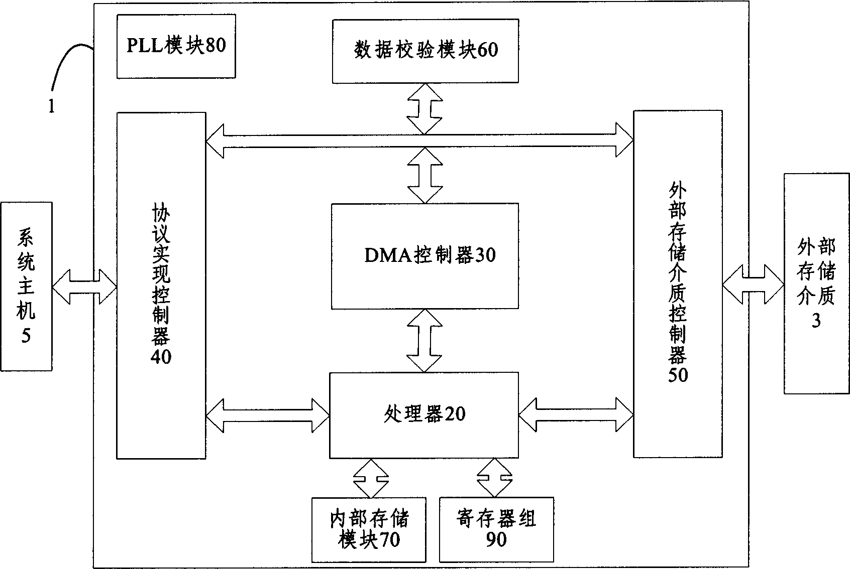
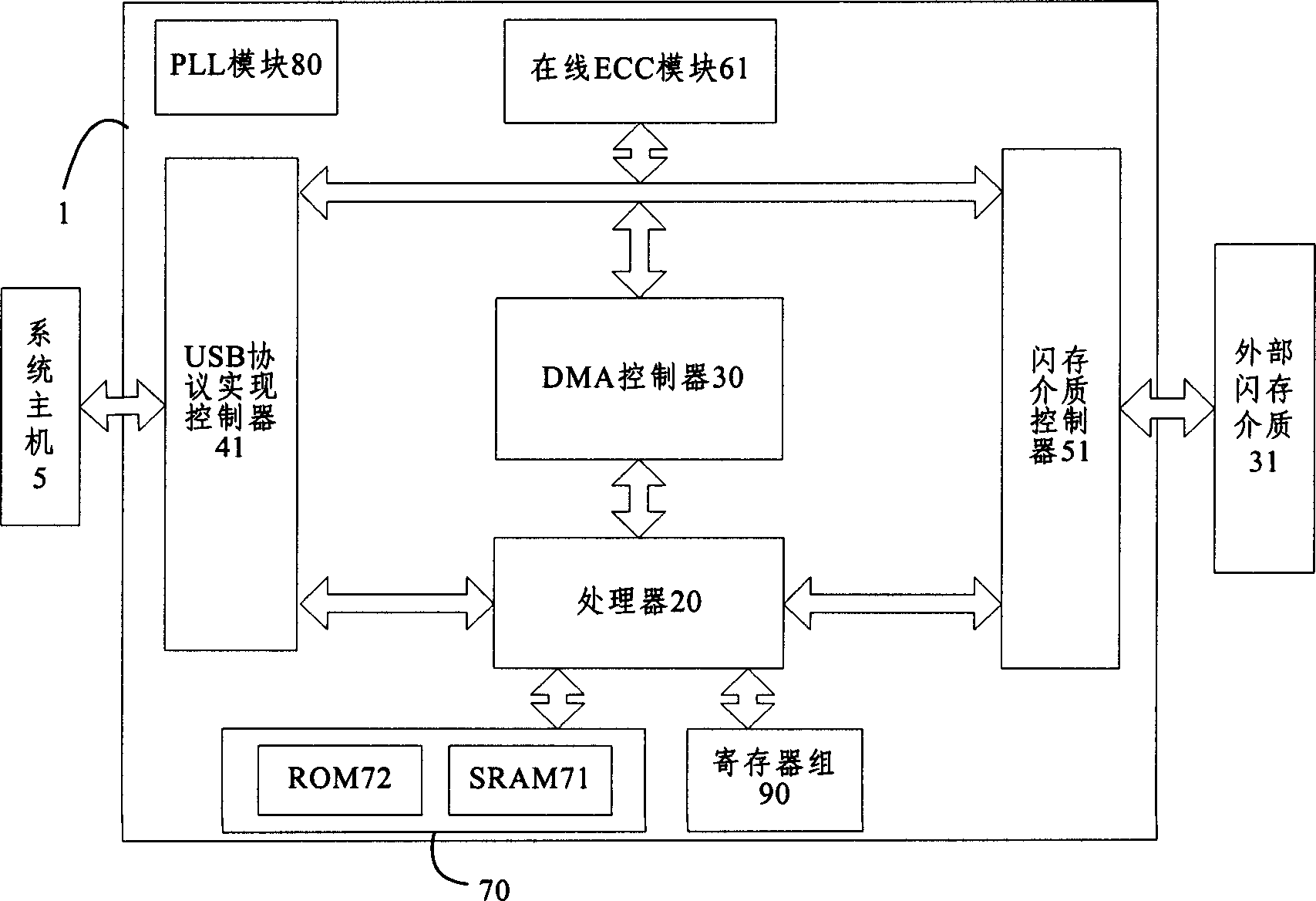
[0030] see figure 1 The storage control chip 1 of the present invention is used to connect the external storage medium 3 and the system host 5, and control data to be transmitted in a large amount, quickly and correctly, and is divided into functional modules, including a processor (MCU) 20, a DMA controller 30, and a protocol A controller 40 , an external storage medium controller 50 , a data verification module 60 , an internal storage module 70 , a PLL module 80 and a register set 90 are realized.

[0031] The external storage medium 3 mentioned here refers to but not limited to SDRAM, DRAM, EPPROM, static random access memory (SRAM), ferromagnetic random access memory / ferroelectric memory (FRAM), magnetoresistive random access memory (MRAM), ultra-high dens...


PUM


Abstract

One kind of memory control chip used for controlling the data access of semiconductor memory medium and the data transmission to the system unit includes processor as the chip controller for data access and transmission and parameter setting; protocol realizing controller connected to the processor to make data transmission coincide with protocol standard; external memory medium controller connected to the processor to control the data access of external memory medium; internal memory module to store the application program and / or system program of the control chip and serve as the buffering memory for data transmission of the control chip; register set with set control parameters and state parameters; DMA controller for quick data transmission; and data verifying module for quick verification in data transmission via on-line coding. The present invention has the advantages of fast, correct and reliable data transmission.

Description

technical field [0001] The invention relates to computer chip technology, in particular to the design of a storage control chip and a method for data storage control. Background technique [0002] The continuous development of semiconductor storage technology has opened up new space for the field of data mobile storage. Due to the advantages of small size, large capacity, high-speed access, easy to carry, stable performance, and not easy to damage, semiconductor storage products have been more and more widely used. In particular, semiconductor storage products with flash memory (FLASHMemoty) as the storage medium have become a mobile storage application for a new generation of personal data, and storage control chips used in this type of semiconductor storage products have become the key to control their data storage. Take the core components. At present, storage control chips widely used at home and abroad include H8S3664 and H8S2215 from Hitachi, ST92163 from ST, and 663...

Claims


Application Information

Patent Timeline
IPC IPC(8): G06F9/00G06F11/10G06F12/00
Inventor 邓国顺成晓华向锋
Owner NETAK TECH KO LTD
Learn More