
Integrated circuit devices having corrosion resistant fuse regions and methods of fabricating the same

A technology of integrated circuit and fuse area, which is applied in semiconductor/solid-state device manufacturing, electric solid-state devices, circuits, etc., and can solve the problem of reduced output of integrated circuit devices

Inactive Publication Date: 2005-02-02
SAMSUNG ELECTRONICS CO LTD
View PDF1 Cites 5 Cited by
  • Summary
  • Abstract
  • Description
  • Claims
  • Application Information

AI Technical Summary

Problems solved by technology

Therefore, damaged or severed tungsten fuses can lead to a significant reduction in the yield of integrated circuit devices in post-repair

Method used


Image

  • Integrated circuit devices having corrosion resistant fuse regions and methods of fabricating the same
  • Integrated circuit devices having corrosion resistant fuse regions and methods of fabricating the same
  • Integrated circuit devices having corrosion resistant fuse regions and methods of fabricating the same

Examples


Embodiment Construction

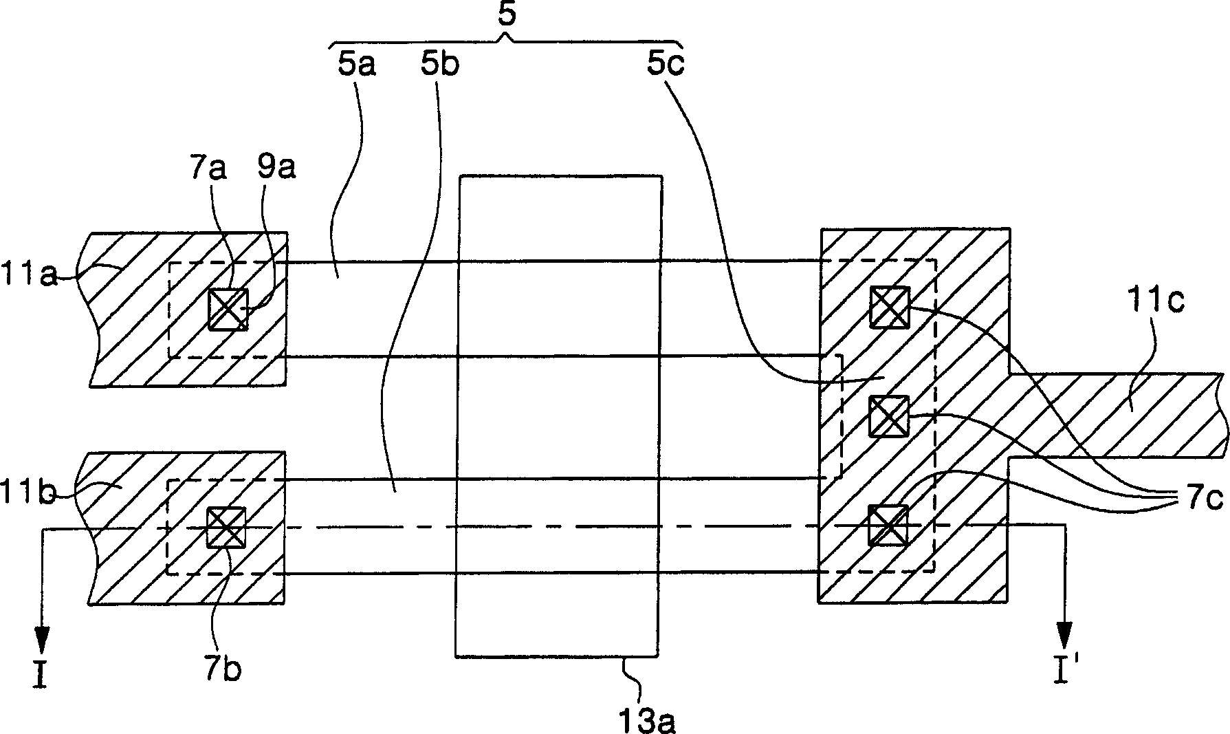
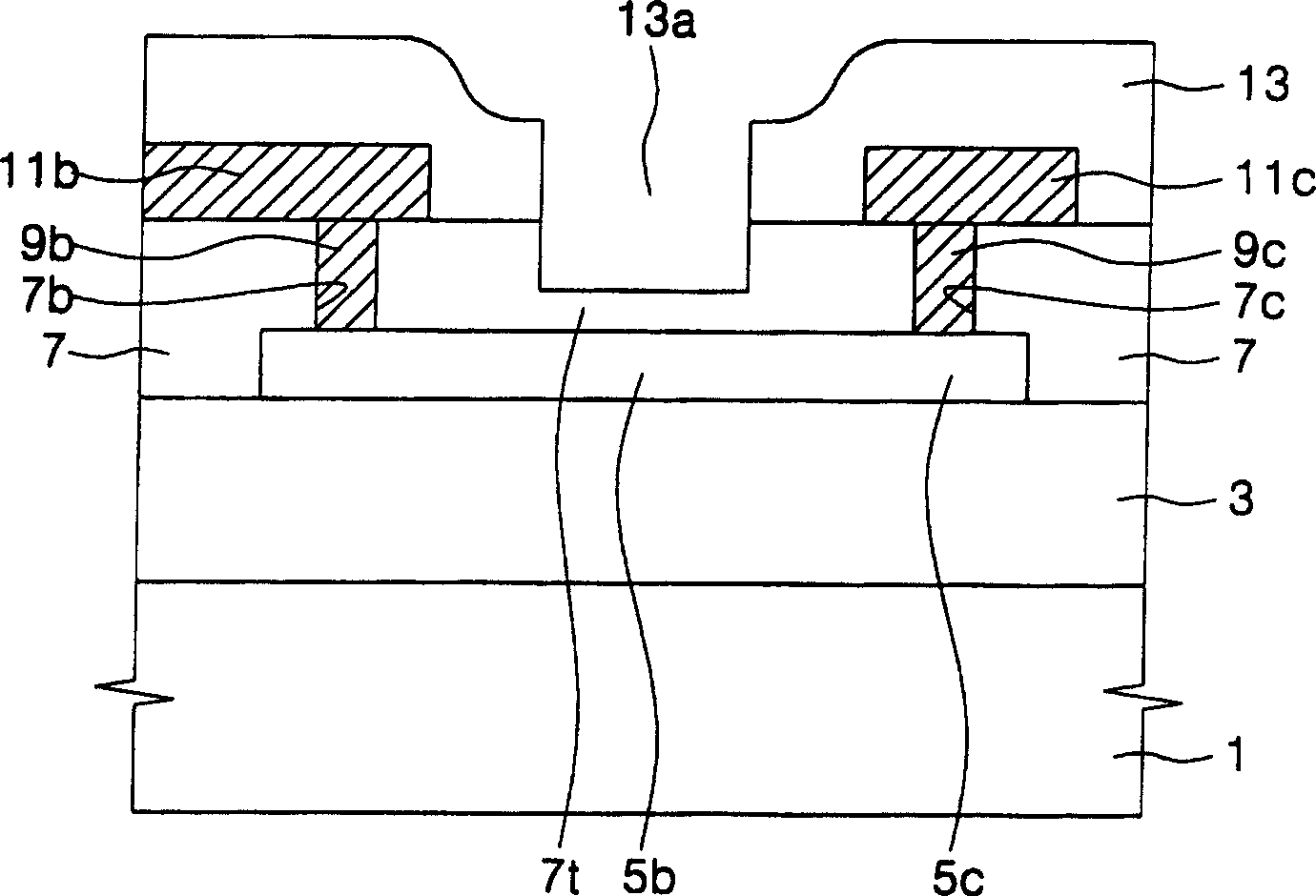
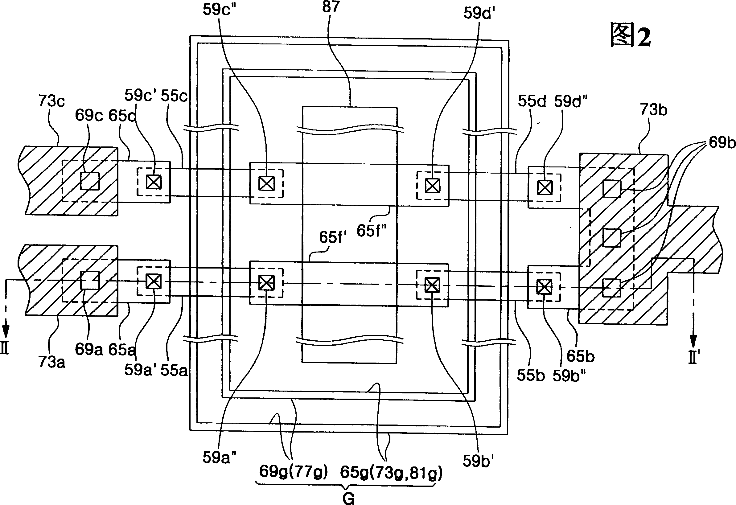
[0036] In the following, the invention will be described more fully with reference to the accompanying drawings, in which preferred embodiments of the invention are shown. Moreover, the invention may be embodied in many different forms and should not be construed as limited to the embodiments set forth herein; rather, these embodiments are set so that these disclosures will be thorough and complete, and will inform the art skilled artisan fully convey the scope of the invention. In the drawings, the thickness of layers and regions are exaggerated for clarity. It will be understood that when a layer is referred to as being on another layer, it can be directly on the other layer or intervening layers may also be present. It will be further understood that when a layer is referred to as being "directly on" another layer, there are no intervening layers. Like numbers refer to like elements throughout. As used herein the term "and / or" includes any and all combinations of one or ...


PUM


Abstract

Integrated circuit devices are provided including an integrated circuit substrate and first through fourth spaced apart lower interconnects on the integrated circuit substrate. The third and fourth spaced apart lower interconnects are parallel to the first and second lower interconnects. A first fuse is provided on the first and second lower interconnects between the first and second lower interconnects and is electrically coupled to the first and second lower interconnects. A second fuse is provided spaced apart from the first fuse and on the third and fourth lower interconnects. The second fuse is between the third and fourth lower interconnects and is electrically coupled to the third and fourth lower interconnects. Related methods of fabricating integrated circuit devices are also provided.

Description

[0001] Refer to related applications [0002] This application is related to and claims priority from Korean Patent Application No. 2003-41249 filed on June 24, 2003, the entire disclosure of which is hereby incorporated by reference. technical field [0003] The invention relates to an integrated circuit device and a manufacturing method thereof, in particular to an integrated circuit device with a fuse area and a manufacturing method thereof. Background technique [0004] Integrated circuit memory devices disposed on integrated circuit substrates are typically tested prior to memory device assembly. In this process, integrated circuit memory devices can be classified as good or bad. If the chip is classified as a bad failure due to one or more failed elements, the failed elements may be replaced by redundant elements already included in the memory device. The repair process may include irradiating a laser beam to blow one or more fuses. Blowing the fuse allows the redun...

Claims


Application Information

Patent Timeline
Patent Type & Authority Applications(China)
IPC IPC(8): H01L23/52H01L21/3205H01L21/82H01L21/822H01L23/525H01L23/58H01L27/04
CPCH01L2924/0002H01L23/585H01L2924/3011H01L23/5258H01L2924/00H01L21/82
Inventor 赵太熙金善俊边光宣慎惠苑姜赫镇
Owner SAMSUNG ELECTRONICS CO LTD
Learn More