Electroluminescent element and its manufacturing method

A technology of electroluminescent components and manufacturing methods, which is applied in the direction of electroluminescent light sources, electrical components, semiconductor/solid-state device manufacturing, etc., and can solve problems such as component characteristic degradation, easy oxidation, and reduced electron injection efficiency

Inactive Publication Date: 2004-12-01
SEIKO EPSON CORP
View PDF1 Cites 3 Cited by
  • Summary
  • Abstract
  • Description
  • Claims
  • Application Information

AI Technical Summary

Problems solved by technology

[0009] However, the above-mentioned alkali or alkaline earth metals are metals with a low work function, so they are very easily oxidized
[0010] Therefore, when producing ITO by the sputtering meth...

Method used


Image

  • Electroluminescent element and its manufacturing method
  • Electroluminescent element and its manufacturing method

Examples


experiment example 1

[0058] Evaluation of the formed organic EL element will be described below by experiment.

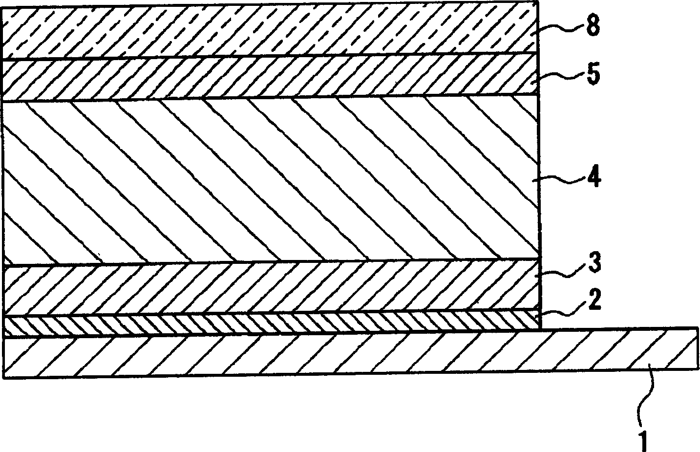
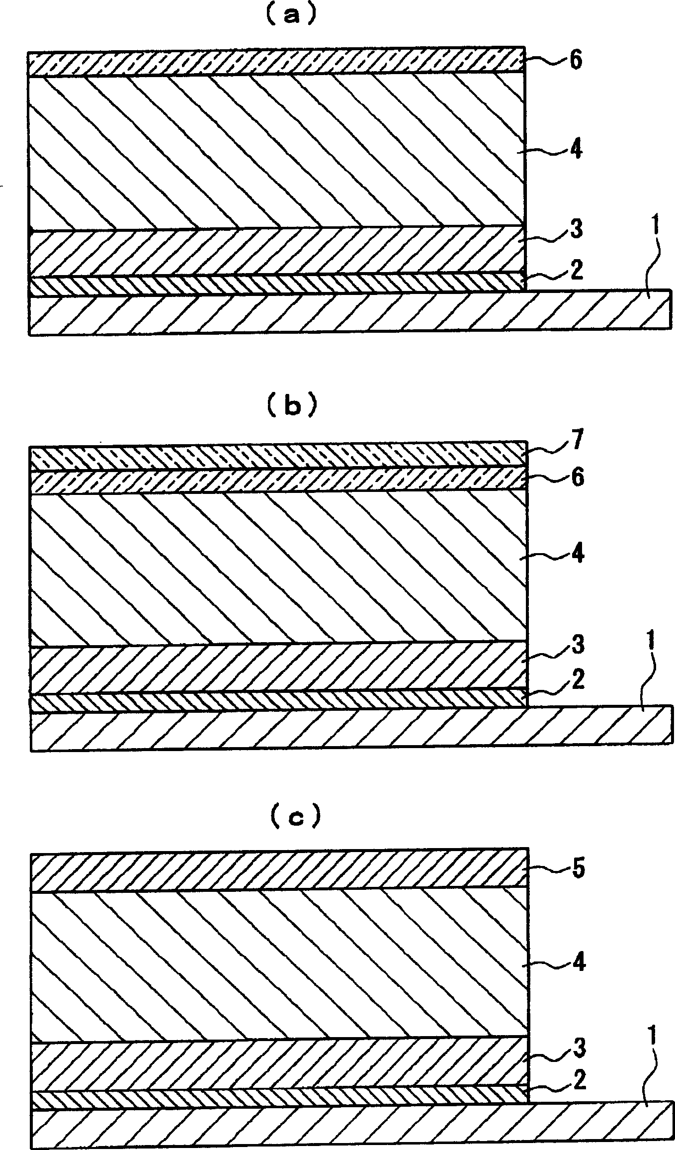
[0059] Here, as an organic EL element, the above-mentioned transparent conductive film 8 is not formed, and a 200 nm thick Al film is vapor-deposited as the reducing metal layer 7, so that the Al film has the function as the reducing metal layer 7 and serves as an electrode (transparent conductive layer 7). Two-sided function of membrane 8). For the film thickness of the metal compound layer 6 , that is, the film thickness of LiF, four types are formed, 0.5 nm; 1 nm; 3 nm; 5 nm. For the electrode 2, a 100 nm thick film was formed with ITO, and for the substrate 1, 1 nm thick ground glass was used. For the hole injection layer 3 and the light emitting layer 4, those shown in the above-mentioned embodiment mode can be used.

[0060] When measuring the luminous intensity of the obtained four organic EL elements, the luminous intensity of the LiF film with a thickness of 0.5nm is 5000cd / m...

experiment example 2

[0063] A LiF film was formed as the metal compound layer 6 with a thickness of 2 nm, 4 nm, 6 nm, 10 nm, and 12 nm, respectively. Other than that, the configuration was the same as in Example 1, and five types of organic EL elements were produced.

[0064] When the luminous efficiency (maximum efficiency) of the obtained five organic EL elements was measured, the luminous efficiency of LiF with a film thickness of 2nm was 9.21m / W, that of 4nm was 6.41m / W, and that of 6nm was 4.41m / W. 10nm is 3.71m / W, and 12nm is considered non-luminous.

[0065] From this result, it is considered that when the metal compound layer 6 is formed thicker than 10 nm, the effect of improving the electron injection property cannot be obtained after the reduction reaction. Therefore, regarding the thickness of the metal compound layer 6, it has been confirmed that 10 nm is preferably taken as its upper limit.


PUM

PropertyMeasurementUnit
Thicknessaaaaaaaaaa
Light intensityaaaaaaaaaa

Abstract

Provided is a top-emission type electroluminescent element in which a total optical transparency of films of the upper part of a light-emitting layer including a transparent conductive film is made to be improved, and in which effective light-emitting intensity can be obtained by improving electron injection efficiency. This organic EL (electroluminescent) element is the top-emission type electroluminescent element, and has a substrate (1), an electrode (2) installed on a surface of the substrate (1), a positive hole injection layer (3) installed on a surface of the electrode (2), a light-emitting layer (4) installed on a surface of the positive hole injection layer (3), a reduction-reacting part (5) installed at the light emitting layer (4), and formed by reduction reaction of an alkaline metal or a metal compound of an alkaline earth metal and a reducer, and a transparent conductive film (8) installed on the reduction-reacting part (5). The reduction-reacting part (5) has a function to demonstrate improvement of the electron injection characteristic to the light emitting layer (4).

Description

technical field [0001] The present invention relates to an electroluminescent element, and more particularly to a structure of a so-called top emission type electroluminescent element that emits light from the top of the element. technical background [0002] Electroluminescent elements (hereinafter referred to as EL) can be used as light-emitting elements for display or lighting, especially organic EL elements that can be used at low voltage, and are expected to be used as extremely power-saving display or light-emitting elements. [0003] The structure of such an organic EL element is generally composed of a structure in which an organic layer is sandwiched between two electrodes. [0004] Conventionally, the so-called bottom-emission organic EL element, which emits light from the side of the glass substrate on which the TFT is formed (the surface of the element connected to the glass substrate), has been widely used. , It is necessary to make a structure that emits light...

Claims


Application Information

Patent Timeline
IPC IPC(8): H05B33/26H01L51/50H01L51/52H05B33/00H05B33/02H05B33/10H05B33/14H05B33/20
CPCH01L2251/5315H01L51/5221H01L51/5092H10K50/171H10K50/82H10K2102/3026F21V17/104
Inventor 深濑章夫
Owner SEIKO EPSON CORP
Why Eureka
Try Eureka