


Quick Research
Generate reliable direction feasibility study reports for your R&D in just a few steps.

Technical Q&A
Discover and master advanced knowledge NOW. Basics, ideas, possibilities, all at once.

Find Solutions
As an expert in R&D theories, this can generate solutions to your technical problems instantly.

Evaluate Feasibility
Analyze your overall solution with one click, know your potential R&D risks in advance.

Monitor Landscape
Get weekly tech updates, stay abreast of the latest tech innovations and key insights.
Semiconductor memory circuit
A storage circuit and semiconductor technology, applied in the direction of semiconductor devices, circuits, information storage, etc., can solve problems such as difficult manufacturing and processing, and achieve the effect of shortening the access time
- Summary
- Abstract
- Description
- Claims
- Application Information
AI Technical Summary
Problems solved by technology
Method used
Image

Examples
Embodiment Construction
[0049] Embodiments of the present invention will be described below with reference to the drawings.
[0050] (Embodiment 1)
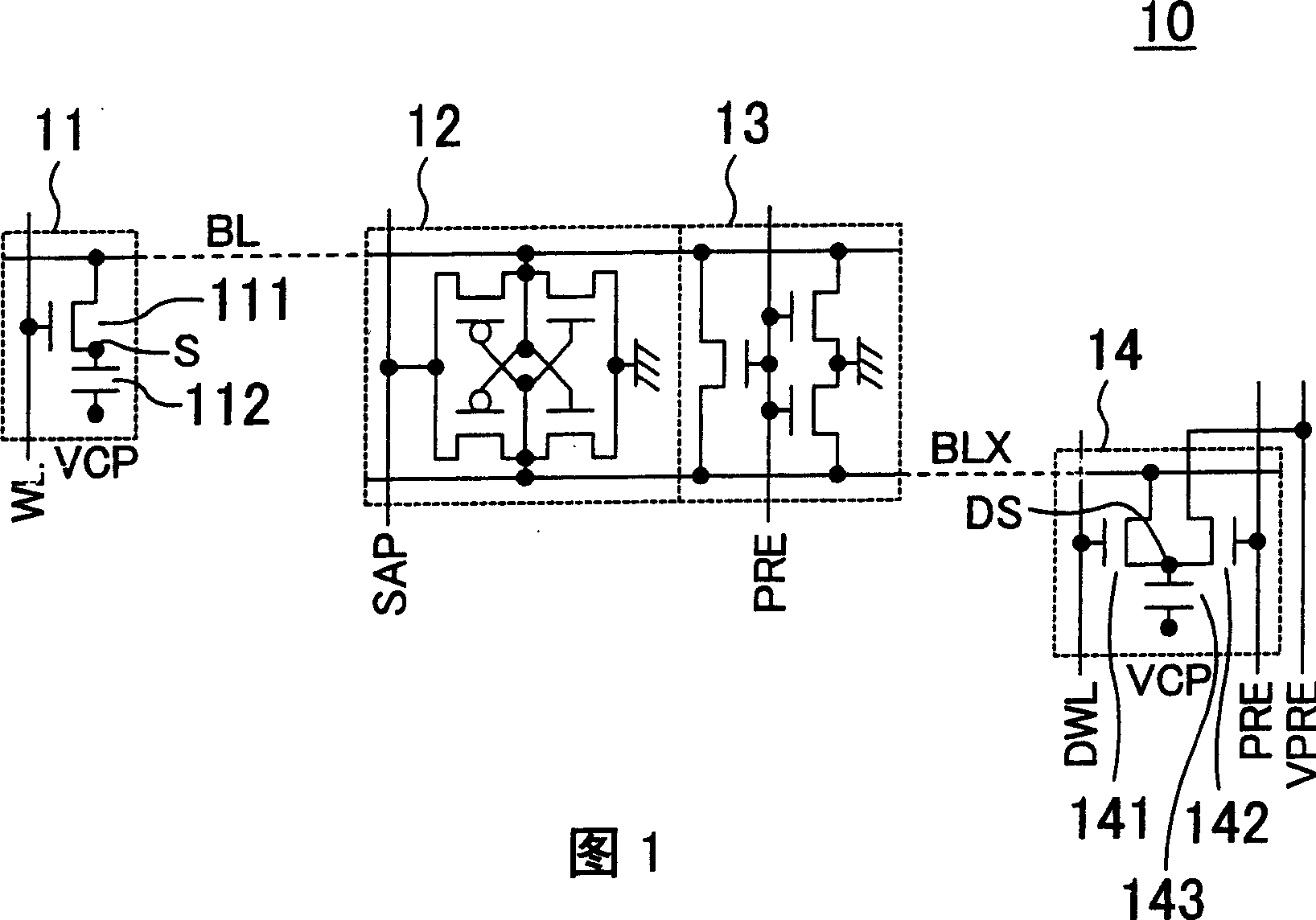
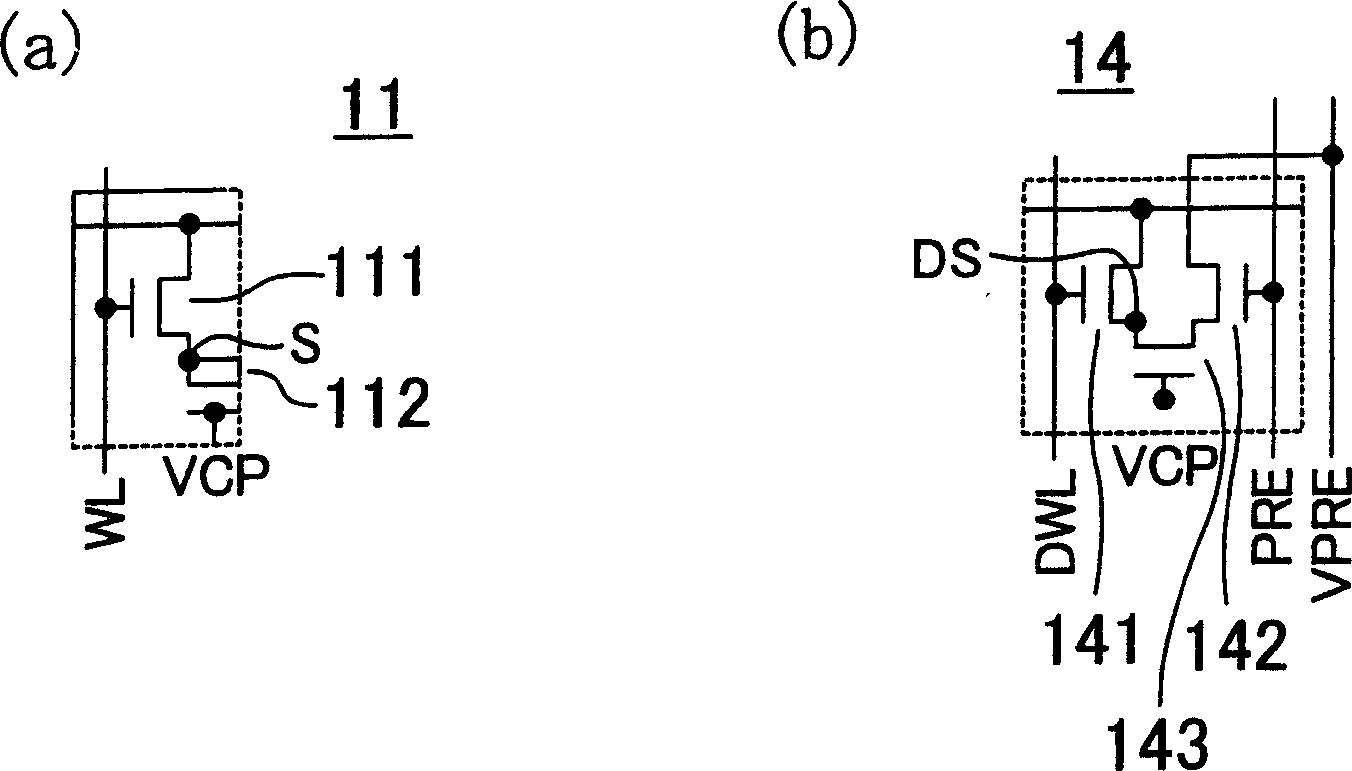
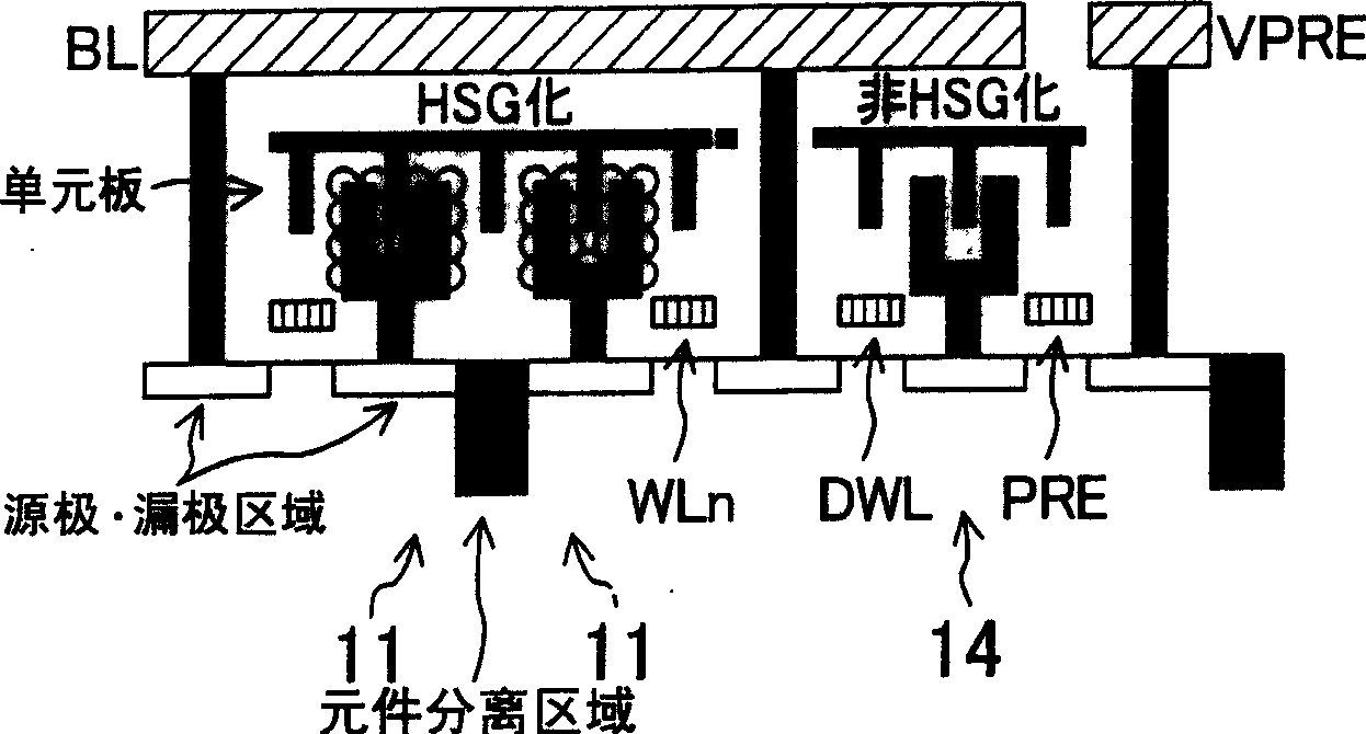
[0051] Fig. 1 shows a circuit configuration of a semiconductor memory circuit according to Embodiment 1 of the present invention. The DRAM 10 as the semiconductor memory circuit of this embodiment is composed of NMOS, and includes a memory cell 11 provided at the intersection of the word line WL and the bit line BL, and a CMOS sense amplifier 12 for detecting and amplifying the potential difference between the pair of bit lines BL and BLX. , a precharge circuit 13 for the bit line pair BL, BLX, and a dummy cell 14 disposed at the intersection of the dummy word line DWL and the bit line BLX.
[0052] The memory cell 11 is a one-transistor type cell constituted by an NMOS transistor 111 and a main capacitor 112 . The NMOS transistor 111 is turned on when the word line WL is activated when the bit line BL is inactive, and electrically connects the main c...
PUM
 Abstract
Description
Claims
Application Information
 - R&D Engineer
- R&D Manager
- IP Professional
- Industry Leading Data Capabilities
- Powerful AI technology
- Patent DNA Extraction
Browse by: Latest US Patents, China's latest patents, Technical Efficacy Thesaurus, Application Domain, Technology Topic, Popular Technical Reports.
© 2024 PatSnap. All rights reserved.Legal|Privacy policy|Modern Slavery Act Transparency Statement|Sitemap|About US| Contact US: help@patsnap.com