


Quick Research
Generate reliable direction feasibility study reports for your R&D in just a few steps.

Technical Q&A
Discover and master advanced knowledge NOW. Basics, ideas, possibilities, all at once.

Find Solutions
As an expert in R&D theories, this can generate solutions to your technical problems instantly.

Evaluate Feasibility
Analyze your overall solution with one click, know your potential R&D risks in advance.

Monitor Landscape
Get weekly tech updates, stay abreast of the latest tech innovations and key insights.
Light emission device
A technology for display devices and transistors, which can be used in identification devices, lighting devices, electroluminescence light sources, etc., and can solve problems such as increased power consumption
- Summary
- Abstract
- Description
- Claims
- Application Information
AI Technical Summary
Problems solved by technology
Method used
Image

Examples
Embodiment approach 1
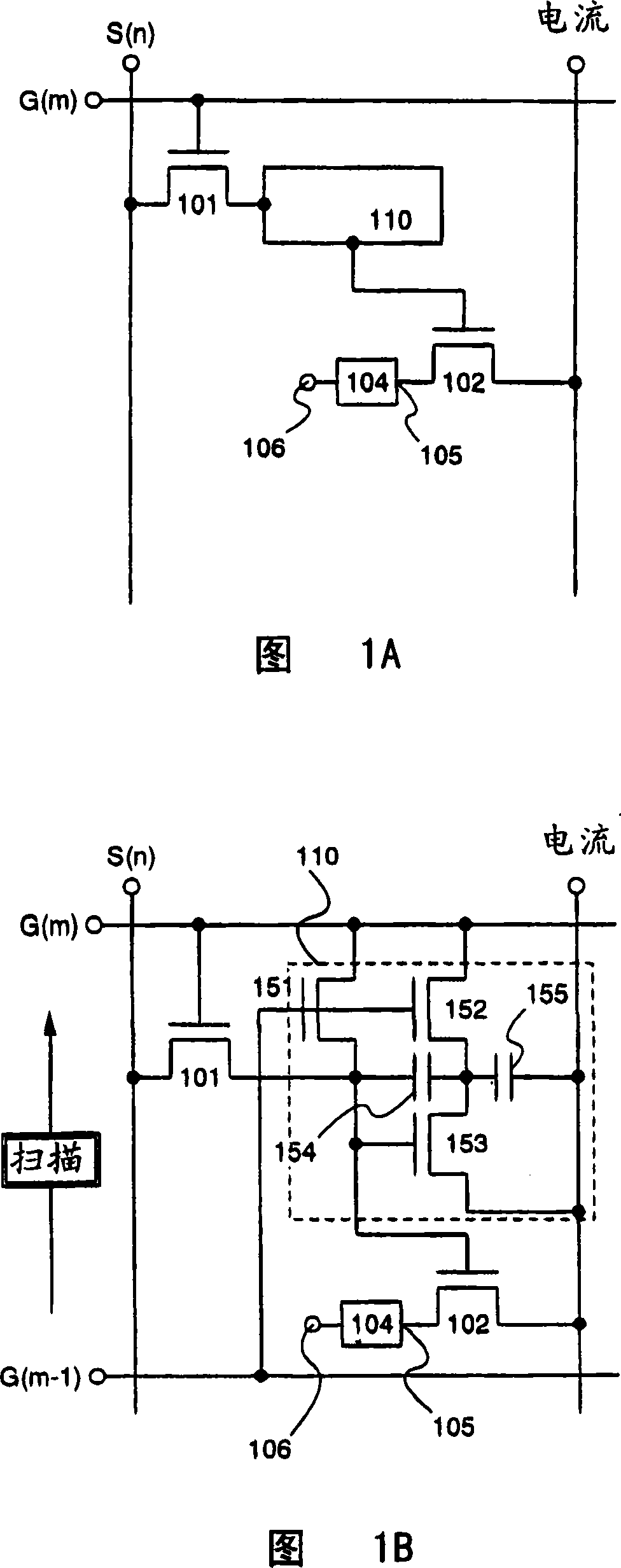
[0138] An example of performing SES driving including an erasing period using pixels with an additional erasing mechanism is described in Embodiment 1.
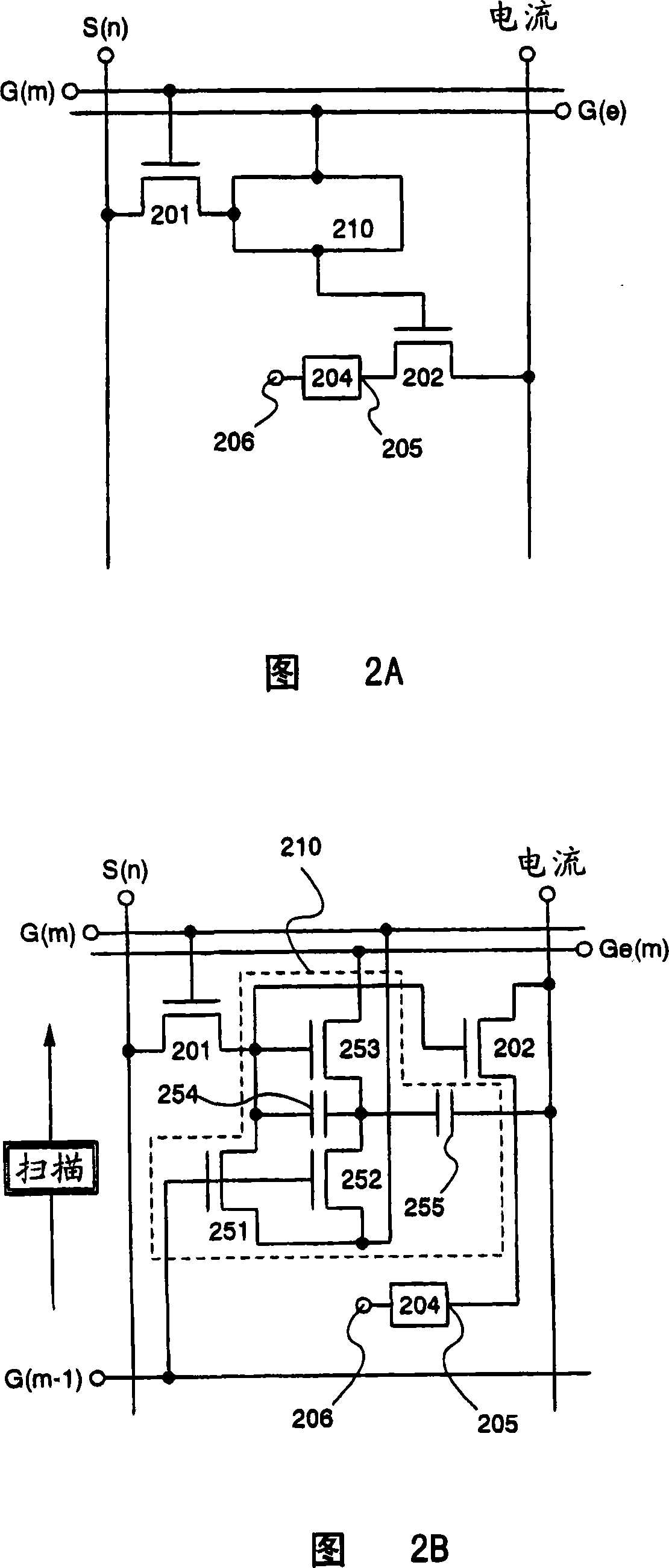
[0139] 2A and 2B illustrate pixel structures with the erasing mechanism of Embodiment 1. FIG. As shown in FIG. 2A, a pixel has a switch TFT 201, a driver TFT 202, an EL element 204, a source signal line (S), a gate signal line (G), and a current supply line (current), which are similar to conventional parts, and have a The voltage compensation circuit 210 of the voltage compensation circuit of Embodiment Pattern 1. In addition to the gate signal line (G), the pixel in Embodiment 1 also has an erasing gate signal line (Ge). Note that referring to the erasing gate signal line (Ge), the conventional gate signal line in Embodiment 1 is referred to as the write gate signal line.
[0140] FIG. 2B is a circuit diagram including the configuration of the voltage compensation circuit 210 . The voltage compensation circuit 210 has a ...
Embodiment approach 2
[0157] An example of manufacturing a light-emitting device having pixels shown in Embodiment Modes 1 and 2 is described in Embodiment 2.
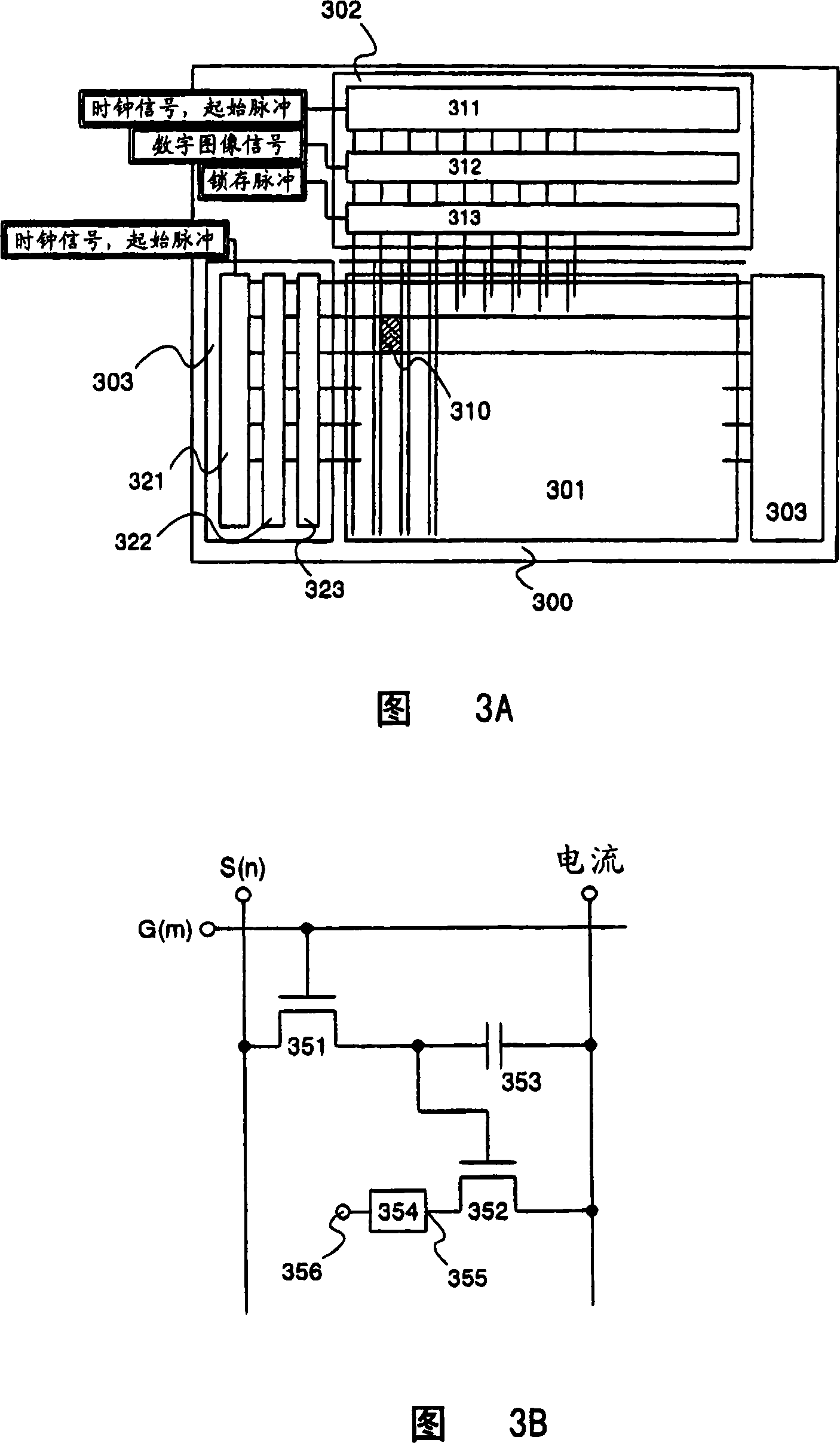
[0158] A schematic diagram of the light emitting device is shown in Figure 20A. A pixel portion 2001 is placed at the central portion of the substrate 2000 . Although not particularly shown in FIG. 20A, the structure of the pixel is the same as that shown in FIGS. 1A and 1B. A source signal line driver circuit 2002 for controlling source signal lines and a gate signal line driver circuit 2007 for controlling gate signal lines are formed around the pixel portion 2001. One of the gate signal line driver circuits 2007 may also be formed only on one side of the pixel portion 2001 as described above.
[0159] Signals input from the outside for driving the source signal line driver circuit 2002 and the gate signal line driver circuit 2007 are input through the FPC 2010 . Signals input from FPC 2010 have small voltage amplitudes, and thus are c...
Embodiment approach 3
[0193] A pixel having an erasing gate signal line is explained in Embodiment 1, but with such a pixel, the selection timing of the writing gate signal line is different from that of the erasing gate signal line. Thus, one of the gate signal line driver circuits disposed on both sides of the pixel portion shown in FIG. 20B can be configured as a write gate signal line driver circuit, and the other can be configured as an erase gate signal line driver circuit. The circuit configuration can be similar to that described in Embodiment 2, and thus its detailed description is omitted here.
PUM
 Abstract
Description
Claims
Application Information
 - R&D Engineer
- R&D Manager
- IP Professional
- Industry Leading Data Capabilities
- Powerful AI technology
- Patent DNA Extraction
Browse by: Latest US Patents, China's latest patents, Technical Efficacy Thesaurus, Application Domain, Technology Topic, Popular Technical Reports.
© 2024 PatSnap. All rights reserved.Legal|Privacy policy|Modern Slavery Act Transparency Statement|Sitemap|About US| Contact US: help@patsnap.com