Semiconductor device4

A semiconductor, conduction technology, applied in the connection/interface layout of logic circuits, reliability improvement of field effect transistors, logic circuits, etc., can solve problems such as hindering high speed and low driving ability

Inactive Publication Date: 2004-10-27
RENESAS ELECTRONICS CORP
View PDF1 Cites 6 Cited by
  • Summary
  • Abstract
  • Description
  • Claims
  • Application Information

AI Technical Summary

Problems solved by technology

[0012] In addition, between the input and output terminals of the input and output buffer circuits ( Figure 15 11) Connect the corresponding drive (for example Figure 15 20) When the driving capability is small, when the input and output buffer circuit switches from the output mode to the input mode, the corresponding driver (such as Figure 15 20) When the output is low level, for example, because the pull-up driving transistor of the input and output buffer circuit (not completely in the off state), there are cases where the input and output terminals are pulled up and the voltage does not drop to low level.
Therefore, when switching from the output mode to the input mode, the output of the tri-state buffer circuit of the input-output buffer circuit becomes a high-impedance state, and it takes a long enough time before the corresponding driver starts to drive, which requires importing the handshake program (bus agreement), which will hinder the high-speed

Method used


Image

  • Semiconductor device4
  • Semiconductor device4
  • Semiconductor device4

Examples


Embodiment Construction

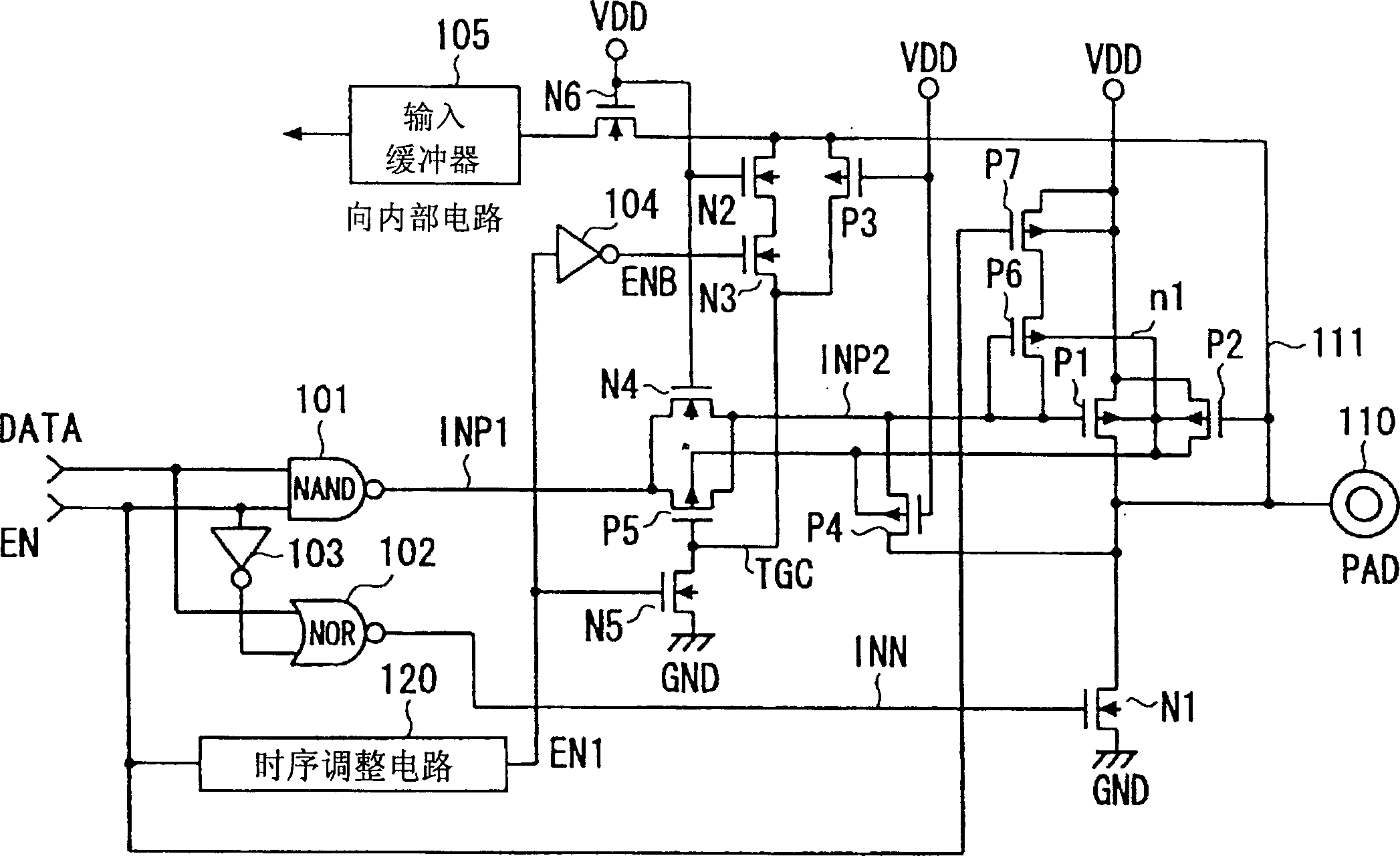
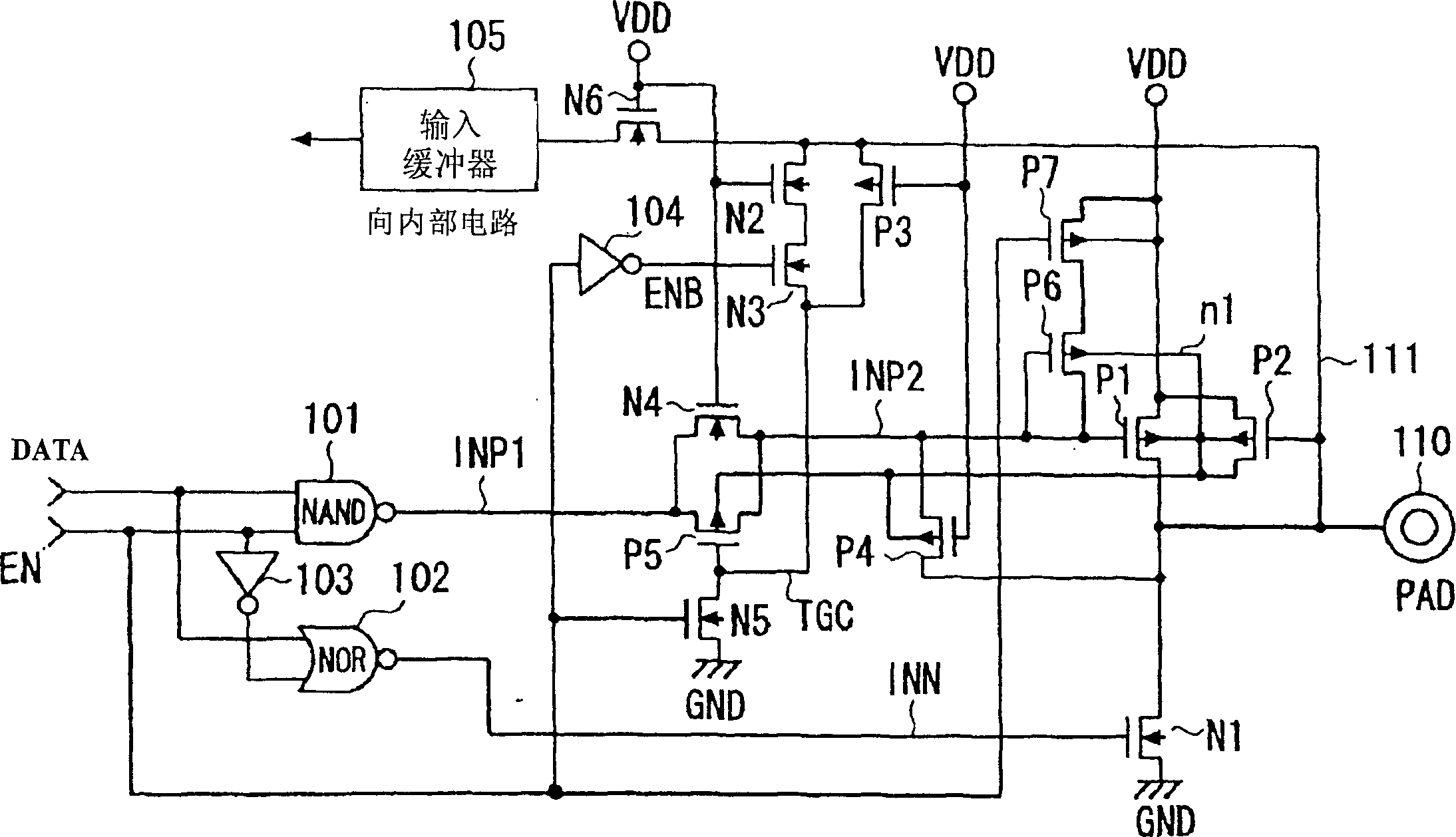
[0033] Embodiments of the present invention will be described below. In a preferred embodiment of the present invention, the semiconductor device has at least a first transistor (P1) for pull-up driving and a second transistor (N1) for pull-down driving in the output stage; When the signal (EN) is a value indicating the enable state, the output is high or low according to the data signal (DATA), and when the control signal (EN) is a value indicating the prohibition state, the output is high impedance state; and has a control unit that performs control such that when the control signal (EN) is switched from the enable state to the prohibit state, the transition of the first transistor (P1) to the cut-off state is accelerated.

[0034] The control unit has the following circuit, which can determine the on / off signal of the first transistor (P1) (such as the signal of the first transistor (P1) when the control signal (EN) is a value indicating the enable state. The signal voltag...


PUM


Abstract

A semiconductor device including a tristate buffer circuit, which includes, on an output stage, at least a first transistor (P1) for pull-up driving and a second transistor (N1) for pull-down driving, in which, when a control signal (EN) is of a value indicating an enable state, an output is set to a high level or to a low level, depending on a data signal, and in which, when the control signal is of a value indicating a disable state, the first and second transistors are turned off to set a high impedance state of the output. The semiconductor device further includes a control unit (120, P6, P7) for performing control for speeding up the transition from the on-state to the off-state of the first transistor (P1) at the time of switching the control signal (EN) from the enable state to the disable state.

Description

technical field [0001] The present invention relates to a semiconductor device, and more particularly, to a mixed voltage circuit that can correspond to a variety of power supply voltages. Background technique [0002] In a semiconductor device or an electronic device having an interface of various power supply systems with different voltages, a three-state snubber circuit (referred to as an "overvoltage-tolerant snubber circuit" or a "mixed voltage circuit") is used. The state buffer circuit allows terminals (pads) connected to the output of the tri-state buffer circuit driven with a relatively low power supply voltage to be connected with terminals of a circuit driven with a relatively high power supply voltage. For example, when connecting the output of the three-state output buffer of a semiconductor device driven by a 3V series power supply to the bus of a system driven by a 5V series power supply, in the input mode (when the output is disabled), make it a three-state o...

Claims


Application Information

Patent Timeline
Patent Type & Authority Applications(China)
IPC IPC(8): G06F3/00H03K19/003H03K19/017H03K19/0175H03K19/094
CPCH03K19/01728H03K19/00315H03K19/09429H03K19/01707
Inventor 北泽元泰铃木康文富田泰弘
Owner RENESAS ELECTRONICS CORP
Why Eureka
Try Eureka