
Method for picking semiconductor chips from a foil

A semiconductor and chip technology, applied in semiconductor devices, semiconductor/solid-state device manufacturing, electric solid-state devices, etc., can solve the problem of not knowing at what height the chip clamp stops

Inactive Publication Date: 2004-06-16
ESEC TRADING
View PDF2 Cites 4 Cited by
  • Summary
  • Abstract
  • Description
  • Claims
  • Application Information

AI Technical Summary

Problems solved by technology

When picking up a semiconductor chip, it brings a problem: since the surface of the semiconductor chip is not at the same height, it is generally unknown at what height the chip clamp stops

Method used


Image

  • Method for picking semiconductor chips from a foil
  • Method for picking semiconductor chips from a foil
  • Method for picking semiconductor chips from a foil

Examples


Embodiment Construction

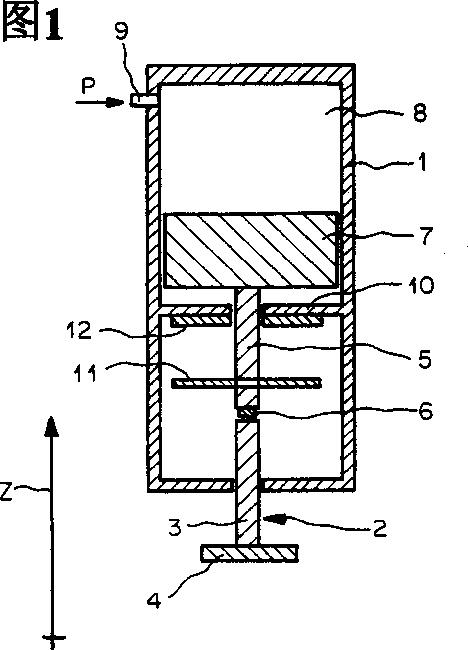
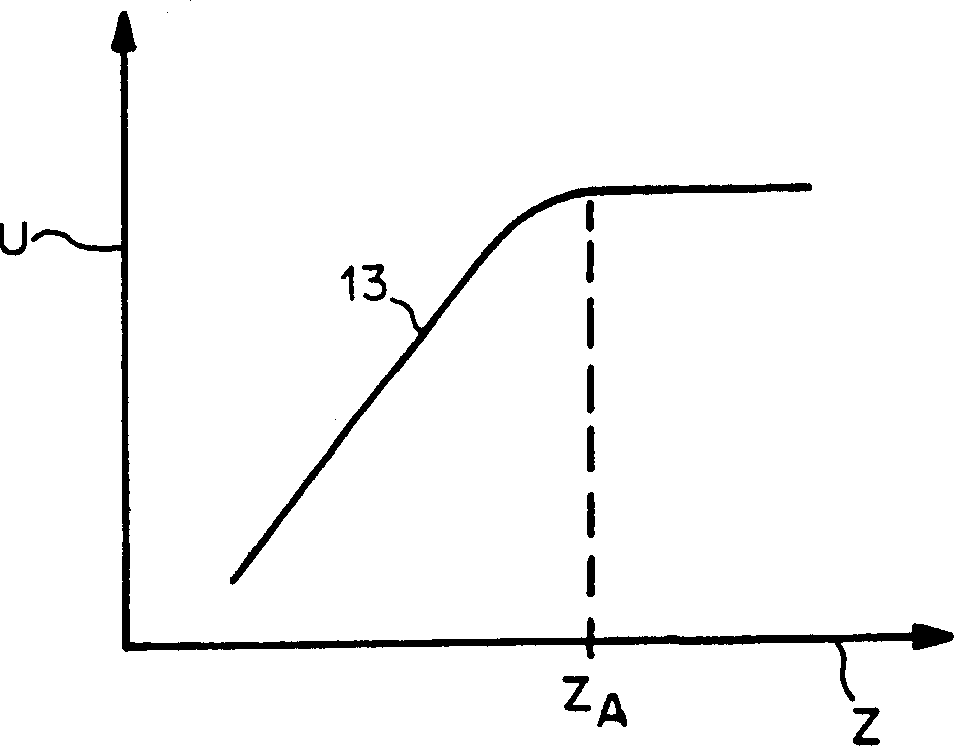
[0024] FIG. 1 shows a first exemplary embodiment of a bonding head 1 of a die bonder, whereby only the elements of the bonding head 1 that are necessary to facilitate the understanding of the invention are shown and described. The bonding head 1 belongs to a pick-and-place system, which serves to pick up semiconductor chips presented on a wafer table and to place them on a substrate. With this embodiment, the bonding head 1 is lowered in a direction designated as the Z direction to pick up the semiconductor chip, then raised again, transferred to the substrate, and lowered again to place the semiconductor chip on the substrate. In order to accurately move the bonded head 1 in the Z direction, the Z position of the bonded head 1 must be measured with an unused driver and an unused measuring system. The drive can lower and raise the bonding head 1 in the Z direction relative to the pick-and-place system or can lower and raise the pick-and-place system and the bonding head 1 toge...


PUM


Abstract

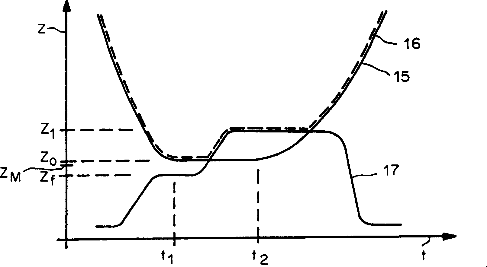
The picking of a semiconductor chip from a foil takes place by means of a chip gripper which bears on a bondhead and can be deflected in a predetermined direction and with the aid of a needle. An inductive sensor serves the precise measurement of the deflection of the chip gripper with reference to the bondhead. The pick process itself is characterised by the following steps: a) Lowering the chip gripper to a height z0, that is greater than an average height of the surface of the semiconductor chips so that the chip gripper does not yet touch the semiconductor chip, b) Raising the needle to a predetermined height z1, whereby the needle raises the semiconductor chip in order to bring the semiconductor chip into contact with the chip gripper and then to increase the height of the chip gripper, and c) Raising the chip gripper, whereby the semiconductor chip detaches itself from the needle.

Description

technical field [0001] The invention deals with a method of picking up semiconductor chips from a foil as stated in the preamble of claim 1 . Background technique [0002] As the semiconductor chip is mounted on the substrate, the substrate is gradually conveyed by the transfer device to a dispensing station on which the attachment is completed, and then to a bonding station on which the next semiconductor chip is placed. The semiconductor chips are attached to foils clamped by frames and placed on so-called wafer stages. Semiconductor chips are picked up one by one from the wafer stage by a device called a pick and place device, transferred and placed on the substrate. The pick-and-place device includes an adhesive head with a chip holder for picking up the semiconductor chip, so that the chip holder can be deflected in a vertical direction against the force relative to the adhesive head. By pick-up force, it is the pick-up force when picking up the semiconductor chip fro...

Claims


Application Information

Patent Timeline
IPC IPC(8): H01L21/50H01L21/00
CPCH01L2221/68322H01L21/67132H01L21/50
Inventor 丹尼尔·博利格尔多米尼克·哈特曼费利克斯·雷欧金·曼哈特
Owner ESEC TRADING
Learn More