IC card
A support and chip technology, applied in the field of personal authentication cards, can solve problems such as IC chip cracking, card damage, and inability to work normally, and achieve the effect of improving bending strength and protecting IC chips
- Summary
- Abstract
- Description
- Claims
- Application Information
AI Technical Summary
Problems solved by technology
Method used
Image
Examples
Embodiment 1
[0121] (production of IC card)
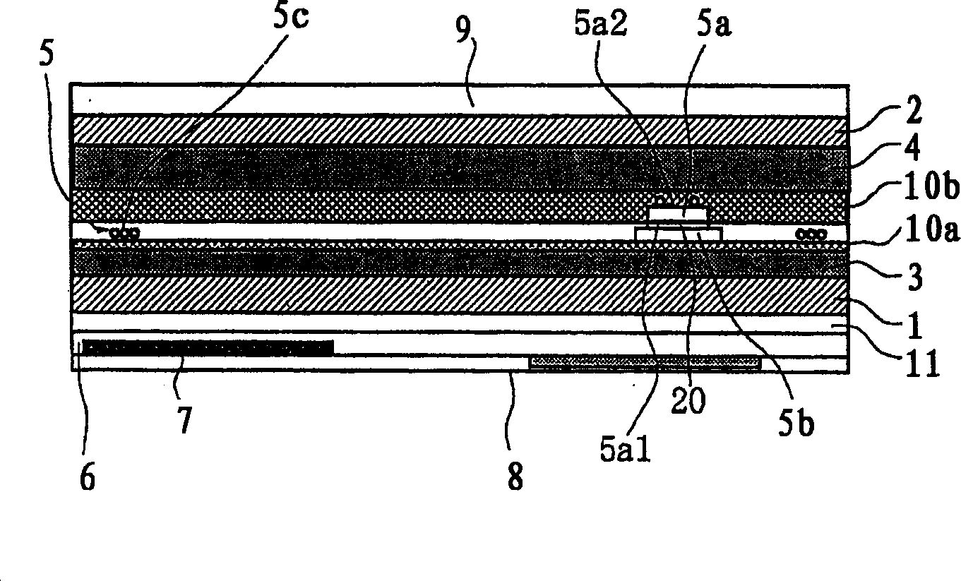
[0122] Figure 10 It is an example of the lamination structure of the IC card and personal authentication card of this invention.
[0123] Support body 1:
[0124] A white polyester sheet with a thickness of 125 μm was used for the first support on the surface side and the second support on the back side.
[0125] Support body 2:
[0126] A white polyester sheet with a thickness of 188 m was used for the first support on the surface side and the second support on the back side.
[0127] (Fabrication of surface-side support)
[0128]
[0129] On the corona discharge treated surface of 125 μm, the first coating solution for forming the imaging layer, the coating solution for forming the second imaging layer, and the coating solution for forming the third imaging layer of the following composition are sequentially coated The coating solution was applied, dried, and stacked to form image-forming layers with respective thicknesses of 0.2 μm, ...
Embodiment 2
[0264] It produced similarly to Example 1 except having used the support body 2 as a front and back support body, and having produced the sheet|seat 2 for IC cards as follows.
[0265] (Production of IC card sheet 2)
[0266] use Figure 11 The above-described card manufacturing apparatus used the aforementioned back support and the surface support having the image-developing layer, which were produced using the support 2 as the first support and the second support.
[0267] Adhesive 1 was applied to a thickness of 34 μm on the first support on the surface side with the imaging layer using a T die, and was applied to a thickness of 34 μm on the second support on the back side using a T die. 300 μm thickness, on the first support on the surface side with the adhesive, place such as Figure 8 IC modules constituted as shown, as Figure 12 It was placed on the second support side with the circuit side on the back side, sandwiched between upper and lower sheets, and laminated a...
Embodiment 3
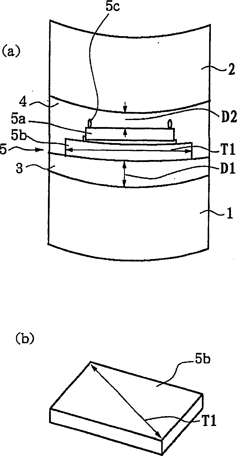
[0272] Except that the IC module was the IC module 2, it produced similarly to Example 2. The thickness D1 of the adhesive between the reinforcing plate and the support was 30 μm, and the ratio of the maximum length T1 of the reinforcing plate as a reinforcing structure was D1 / T1=0.004. The thickness D2 of the adhesive between the IC chip and the support was 149 μm, and the ratio to the maximum length T1 of the reinforcing plate as the reinforcing structure was D2 / T1=0.021.
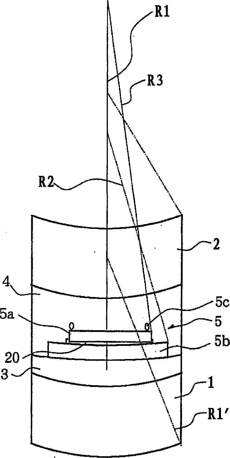
[0273] After the produced IC card was strongly rolled into a cylinder with R = 25mm in the long side direction, the front side and the back side were each strongly rolled and fixed for 24 hours, the IC worked normally. After 100 repeated bending tests, there is no deformation and the IC works normally. A load of 1 kg was applied 10 times to a rubber sheet with a hardness of 50 on each of the circuit surface and the non-circuit surface of the IC chip with a steel ball with a tip diameter R=1mm, and no dam...
PUM
| Property | Measurement | Unit |
|---|---|---|
| thickness | aaaaa | aaaaa |
| thickness | aaaaa | aaaaa |
| thickness | aaaaa | aaaaa |
Abstract
Description
Claims
Application Information
 - R&D
- Intellectual Property
- Life Sciences
- Materials
- Tech Scout
- Unparalleled Data Quality
- Higher Quality Content
- 60% Fewer Hallucinations
Browse by: Latest US Patents, China's latest patents, Technical Efficacy Thesaurus, Application Domain, Technology Topic, Popular Technical Reports.
© 2025 PatSnap. All rights reserved.Legal|Privacy policy|Modern Slavery Act Transparency Statement|Sitemap|About US| Contact US: help@patsnap.com


