
Design method of semiconductor chip

A chip design, semiconductor technology, applied in the direction of semiconductor devices, semiconductor/solid-state device manufacturing, CAD circuit design, etc., can solve the problem of increasing the number of level shifters

Inactive Publication Date: 2002-06-12
IBM CORP
View PDF0 Cites 18 Cited by
  • Summary
  • Abstract
  • Description
  • Claims
  • Application Information

AI Technical Summary

Problems solved by technology

However, having to distribute different power and logic clusters everywhere greatly increases the number of level shifters

Method used


Image

  • Design method of semiconductor chip
  • Design method of semiconductor chip
  • Design method of semiconductor chip

Examples


Embodiment Construction

[0019] As noted above, the present invention relates to computer-aided circuit layout on semiconductor chips. For those unfamiliar with the subject, the following overview section briefly introduces some of the concepts related to the layout process. Those skilled in the art of computer-aided circuit layout on semiconductor chips will wish to proceed directly to the details.

[0020] review

[0021] In designing semiconductor chips, computer design tools are used. These tools work and produce a file called a netlist. This netlist contains a description of all gates and the connections between them. Semiconductor chip designers typically work with an analog logic layout of the chip. In other words, the semiconductor chip will perform a certain function, and the designer ensures that the analog chip actually logically performs that function. When the actual chip is ready to be fabricated, the designer uses a layout tool that takes the original netlist and produces the outpu...


PUM


Abstract

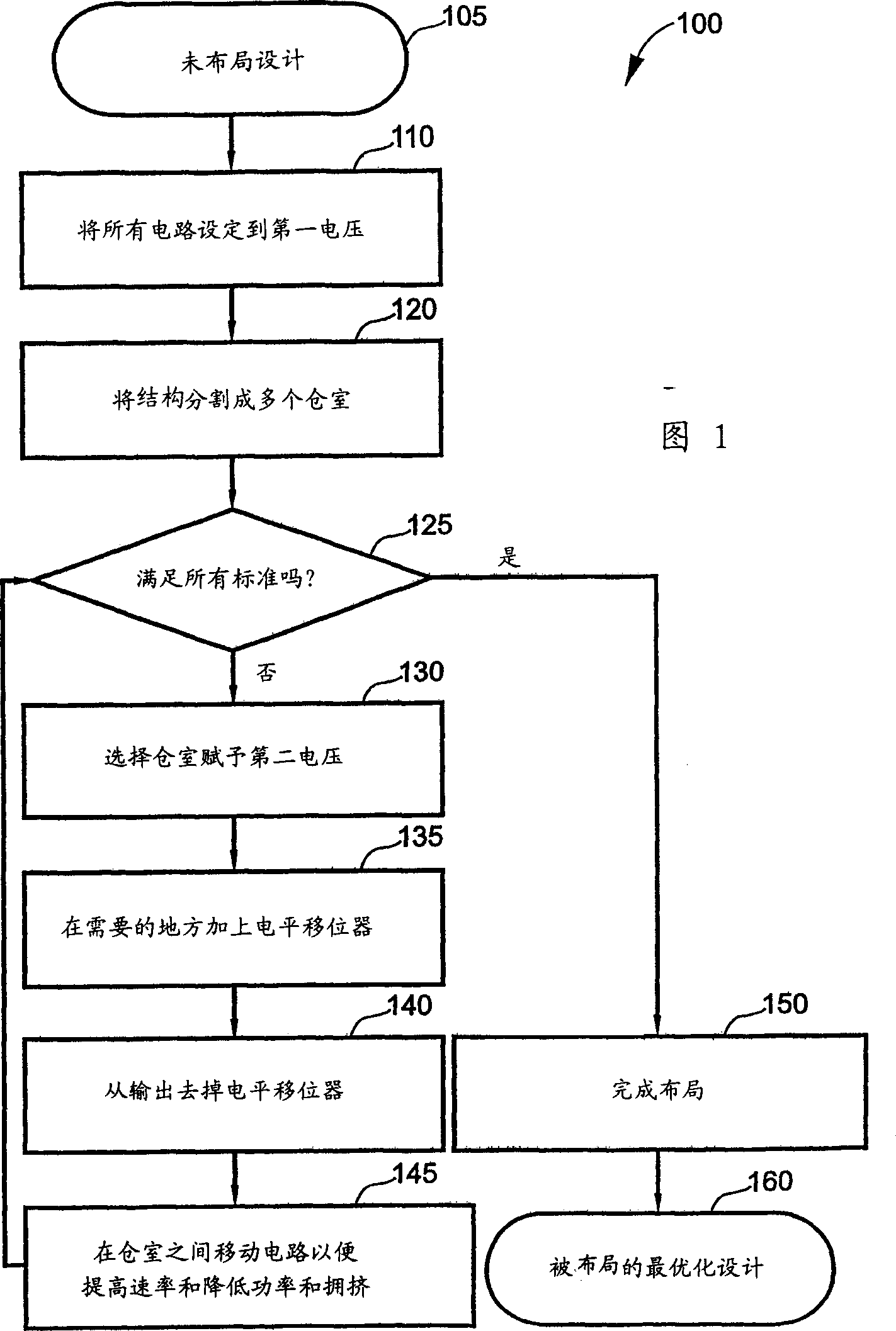
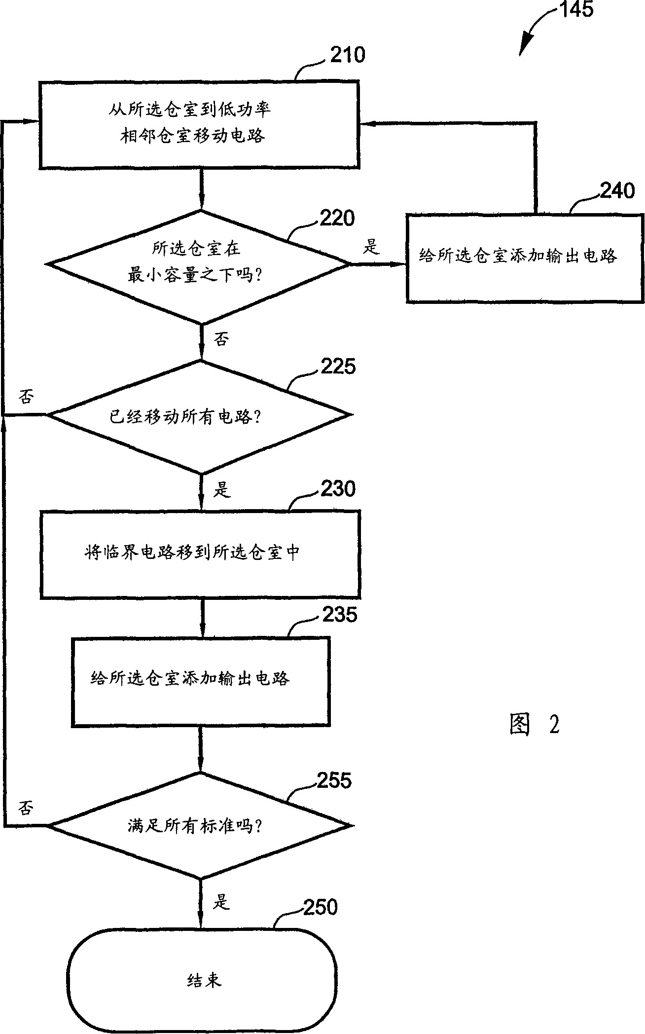
Both logical and physical construction of voltage islands is disclosed. A semiconductor chip design is partitioned into 'bins', which are areas of the design. In this way, a semiconductor chip design may be 'sliced' into various areas and the areas may then be assigned to various voltage levels. Each bin may be thought of as a voltage island. Circuits in the design can be added to or removed from the various bins, thereby increasing or decreasing the speed and power of the circuits: the speed and power increase if a circuit is placed into a bin assigned a higher voltage, and the speed and power decrease if a circuit is placed into a bin having a lower voltage. The size and location of the bins may also be changed. By iterating these steps, the optimum power consumption may be met while still meeting speed constraints and other criteria. The present invention is applicable to any placement environment, such as an annealing placement tool, that proceeds through successive refinement of the locations of the circuits on the design and in which the placement process may be interrupted to make changes in placement of the logic.

Description

technical field [0001] The present invention relates generally to computer aided circuit placement on semiconductor chips, and in particular to parallel logical and physical structures of voltage islands for mixed supply voltage designs. Background technique [0002] The conversion power of digital circuits increases with the square of the supply voltage. Thus, reducing this voltage is required to reduce circuit power consumption. However, reducing the supply voltage also degrades circuit performance. Therefore, it is required to combine circuits driven by a higher power supply voltage and circuits driven by a lower power supply voltage (hereinafter referred to as high and low voltage circuits, respectively) on the same chip. Use high voltage circuits where needed to achieve the desired circuit performance and low voltage circuits elsewhere. [0003] When high and low voltage circuits are combined on one semiconductor chip in this way, it is requir...

Claims


Application Information

Patent Timeline
Patent Type & Authority Applications(China)
IPC IPC(8): G06F17/50H01L21/82
CPCG06F17/5045G06F17/5068G06F30/39G06F30/30
Inventor 约翰·M·科恩阿尔瓦·A·迪安戴维·J·哈萨卫戴维·E·拉基托马斯·M·莱普西克苏珊·K·利希滕斯泰格斯科特·A·泰特劳尔特塞巴斯蒂安·T·文特伦
Owner IBM CORP
Learn More