Liquid crystal display device
A liquid crystal display device, liquid crystal technology, applied in nonlinear optics, instruments, optics, etc., can solve the problems of large size, large size of mobile phone main body 100, poor appearance design effect, etc., and achieve the effect of preventing corrosion
- Summary
- Abstract
- Description
- Claims
- Application Information
AI Technical Summary
Problems solved by technology
Method used
Image
Examples
no. 2 Embodiment
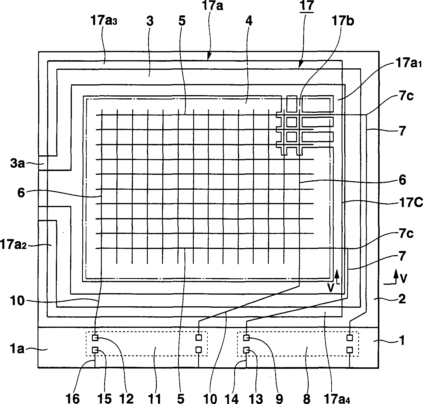
[0065] In the first embodiment above, if figure 1 As shown, the case where the lead wire 7 is arranged only on the right side portion of the active substrate 1 is described, but it is not limited to this. For example it can also be like Image 6As shown in the second embodiment of the present invention. That is to say, in this embodiment, the semiconductor integrated circuit device 11 for data line driving is installed in the center on the lower side protrusion 1a of the active substrate 1, and the semiconductor integrated circuit device 11 for scanning line driving is installed on the left and right sides thereof. Devices 8A and 8B. And, the right end portion of about 1 / 2 of the upper side in the scanning signal line 5 is connected to the output side connection terminal 9A of the semiconductor integrated circuit device 8A for driving the scanning line through the lead line 7b1 arranged on the right side thereof, This semiconductor integrated circuit device 8A is mounted o...
no. 3 Embodiment
[0074] In the above-mentioned second embodiment, the semiconductor integrated circuit device 11 for data line driving is described in the central part on the lower side protrusion 1a of the active substrate 1, and the semiconductor integrated circuit device 8A for scanning line driving is described. The case where 8B is installed on its left and right positions. However, the present invention is not limited thereto. For example, if a semiconductor integrated circuit employs a driver circuit capable of driving both scanning signal lines and data signal lines, then only one semiconductor integrated circuit device is mounted on the active substrate 1 . Figure 8 The illustrated third embodiment of the invention represents such an embodiment. On the lower protruding portion 1a of the active substrate 1, a semiconductor integrated circuit device 31 for data line driving and scanning line driving is mounted. exist Figure 8 Among them, 41 is a flexible printed circuit board bonded...
no. 4 Embodiment
[0076] In the above-mentioned second embodiment, the case where only the lower edge portion of the active substrate 1 protrudes from the counter substrate 2 has been described, but the present invention is not limited to this. For example, it is also possible to Figure 9 As shown in the fourth embodiment of the present invention. In this embodiment, the lower portion and the upper portion of the active substrate 1 are protruded from the opposite substrate 2, and the semiconductor integrated circuit device 33 for driving the data lines is mounted on the central portion of the lower protruding portion 1a. A semiconductor integrated circuit device 34 is mounted to the central portion of the upper side protrusion 1b.
[0077] In this case, about 1 / 2 part of the upper side in the scanning signal line 5, its right end portion is connected to the output side connection terminal (not shown in the figure) of the semiconductor integrated circuit device 34 through the lead wire 27a tha...
PUM
 Abstract
Description
Claims
Application Information
 - R&D Engineer
- R&D Manager
- IP Professional
- Industry Leading Data Capabilities
- Powerful AI technology
- Patent DNA Extraction
Browse by: Latest US Patents, China's latest patents, Technical Efficacy Thesaurus, Application Domain, Technology Topic, Popular Technical Reports.
© 2024 PatSnap. All rights reserved.Legal|Privacy policy|Modern Slavery Act Transparency Statement|Sitemap|About US| Contact US: help@patsnap.com


