Method of forming semiconductor device
A manufacturing method and semiconductor technology, applied in the fields of semiconductor/solid-state device manufacturing, semiconductor devices, chemical instruments and methods, etc., can solve the problems such as the impossibility of improving the interface steepness, the undiscovered mobility, and the decrease of gm, and achieve epitaxy Steep interface, increased fT, increased gm effect
- Summary
- Abstract
- Description
- Claims
- Application Information
AI Technical Summary
Problems solved by technology
Method used
Image
Examples
Embodiment 1
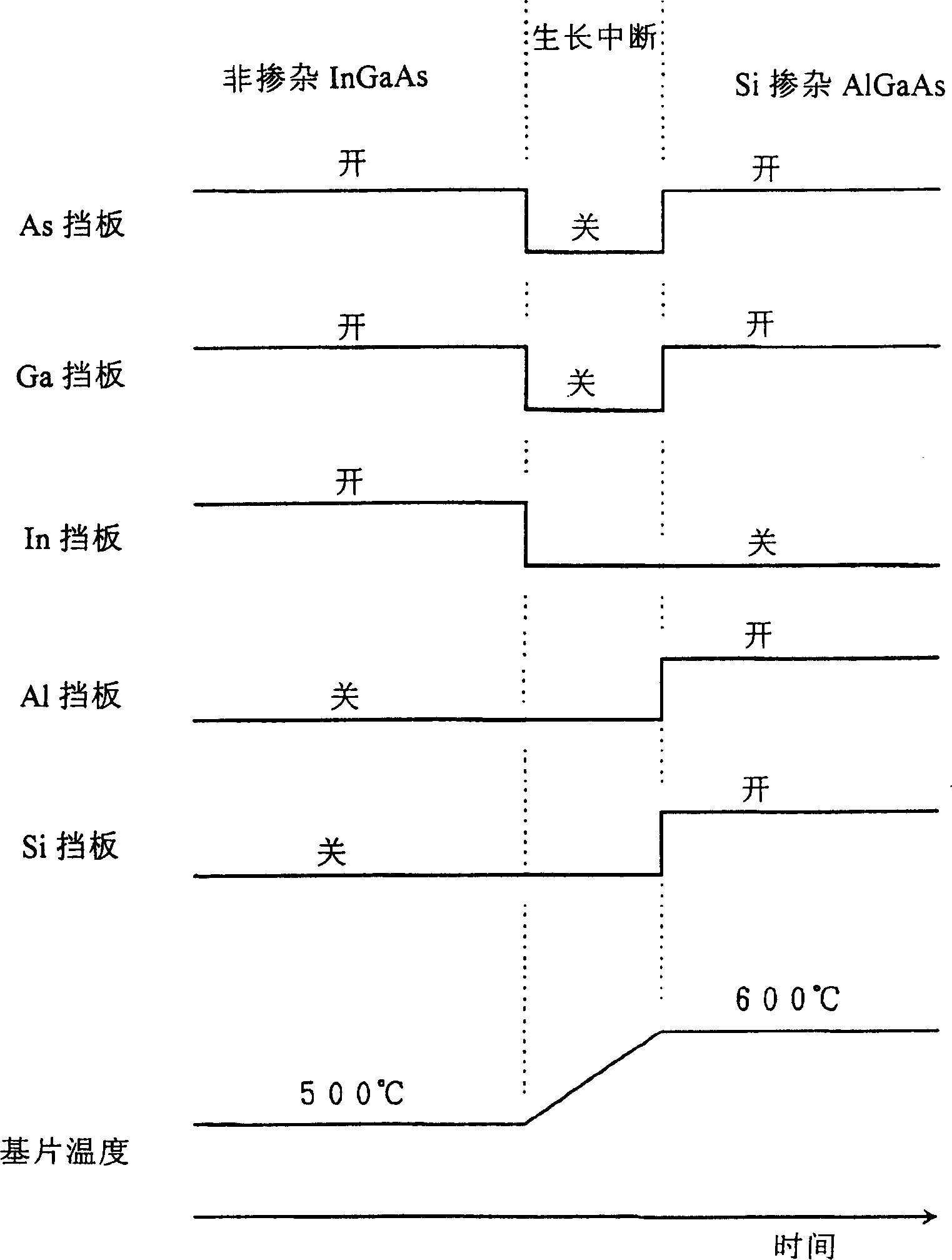
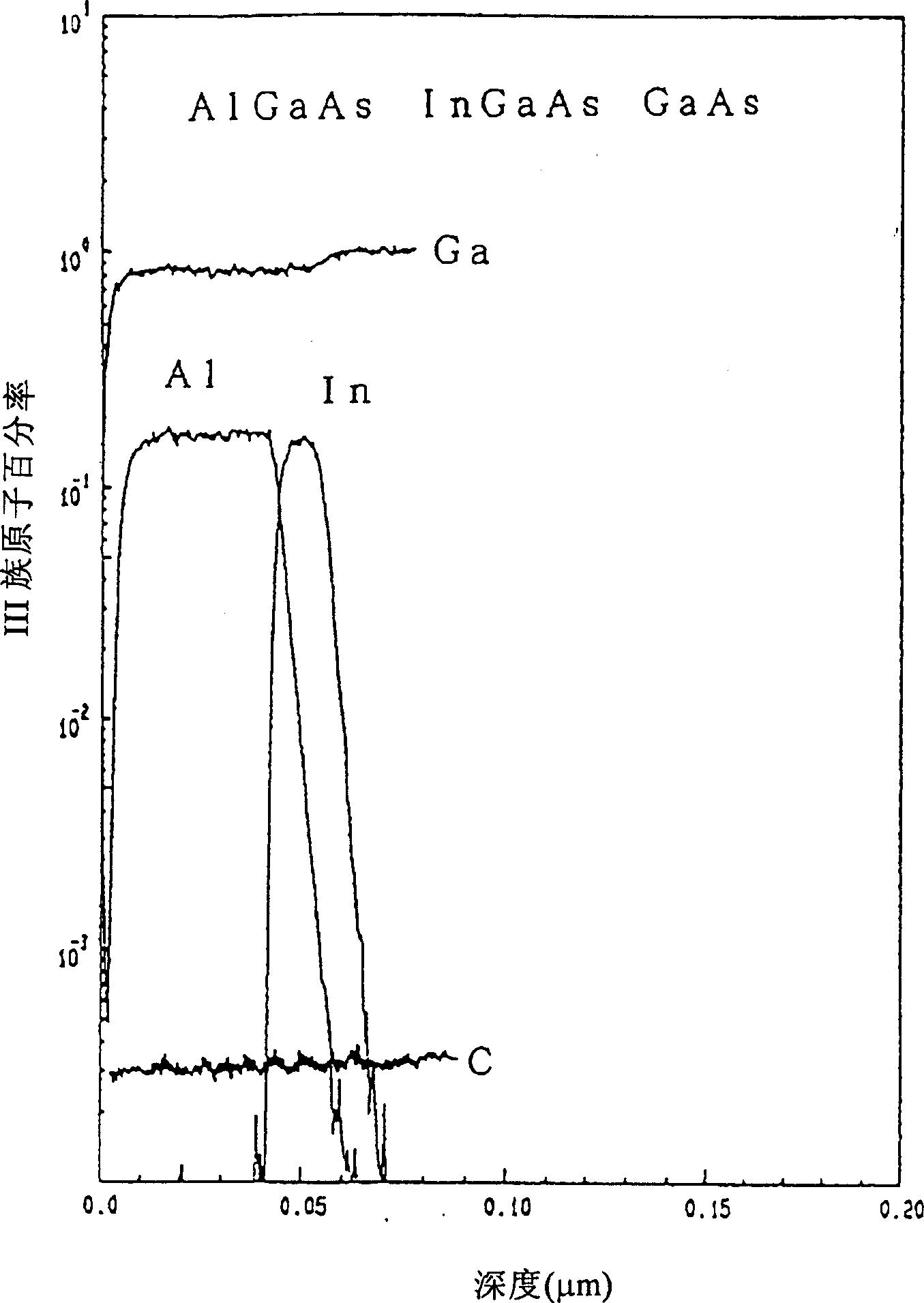
[0025] Below, explain figure 1 Example shown. First, in figure 1 Before the structure growth of the GaAs substrate 11 is cleaned, a cleaning process of 630° C. for 15 minutes is performed, and then a 0.5 μm non-doped GaAs buffer layer 12 is grown at a substrate temperature of 600° C. down to 500°C, grow 15nm non-doped In 0.15 Ga 0.85 As channel layer 13, growing In 0.15 Ga 0.85After the As channel layer 13, the supply of In, Ga, and As was stopped (the growth was temporarily stopped), and at the same time, the substrate temperature was raised to 600°C. During this temperature rise period, remaining In of the InGaAs layer is evaporated. Since the remaining In does not provide As, it can be evaporated by breaking the bond with As, so the evaporation rate is increased, and the remaining In can be removed from the surface of the InGaAs channel layer in a short time. Since the stop time is about 45 seconds and there is no hold time, it is shorter than the conventional one ...
Embodiment 2
[0030] Figure 4 is a cross-sectional view showing an embodiment of the present invention in which planar doping is performed. In the figure, 21 represents the non-doped GaAs substrate, 22 represents the non-doped GaAs buffer layer, and 23 represents the non-doped In 0.2 Ga 0.8 As channel layer, 24 means non-doped Al 0.2 Ga 0.8 As liner layer, 25 means Si planar doped layer, 26 means non-doped Al 0.2 Ga 0.8 As blocking layer, 27 represents a Si-doped GaAs spacer layer, 28 represents a gate, 29 represents a source, and 30 represents a drain.
[0031] In this embodiment, before the start of the growth, the GaAs substrate 21 is cleaned at 630° C. for 10 minutes, and then a 0.5 μm non-doped GaAs buffer layer 22 is grown at a substrate temperature of 600° C. , lower the substrate temperature to 500°C, grow 10nm non-doped In 0.2 Ga 0.8 As channel layer 23, growing In 0.2 Ga 0.8 After the As channel layer 23, the supply of In, Ga, and As is stopped, and the growth is tempor...
PUM
 Abstract
Description
Claims
Application Information
 - Generate Ideas
- Intellectual Property
- Life Sciences
- Materials
- Tech Scout
- Unparalleled Data Quality
- Higher Quality Content
- 60% Fewer Hallucinations
Browse by: Latest US Patents, China's latest patents, Technical Efficacy Thesaurus, Application Domain, Technology Topic, Popular Technical Reports.
© 2025 PatSnap. All rights reserved.Legal|Privacy policy|Modern Slavery Act Transparency Statement|Sitemap|About US| Contact US: help@patsnap.com


