Non-volatility internal memory structure

A non-volatile memory technology, applied in electrical components, electric solid-state devices, circuits, etc., can solve serious problems such as increased power consumption of non-volatile memory components, affecting the accuracy of data reading, etc., to reduce power consumption volume effect

Inactive Publication Date: 2006-11-22
MACRONIX INT CO LTD
View PDF0 Cites 0 Cited by
  • Summary
  • Abstract
  • Description
  • Claims
  • Application Information

AI Technical Summary

Problems solved by technology

However, when the channel length shrinks, the Short Channel Effect (SCE) will be more serious, and the drain-turn-on leakage (DTOL) will also increase significantly
This will affect the accuracy of data reading and increase the power consumption of non-volatile memory components

Method used


Image

  • Non-volatility internal memory structure
  • Non-volatility internal memory structure
  • Non-volatility internal memory structure

Examples


Embodiment Construction

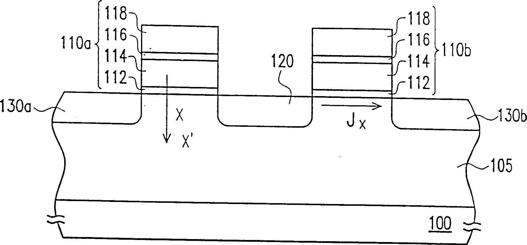
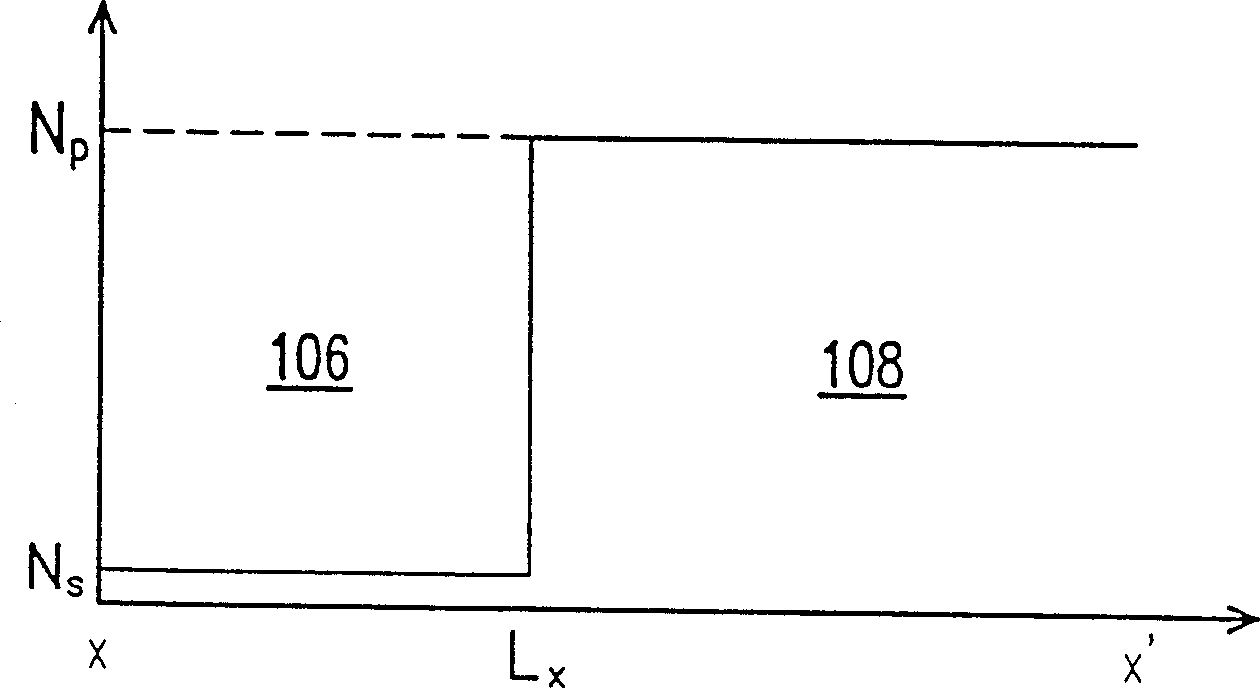
[0020] Please refer to figure 1 , Figure 1A , is the structure of the dual memory unit (Dual-cell) non-volatile memory of the embodiment of the present invention, wherein Figure 1A Shows the vertically stepped channel doping profile (VLCP) in the substrate. like figure 1 As shown, this structure includes a substrate 100, a well region 105 located in the substrate 100, two stacked gate structures 110a and 110b located on the substrate 100, and a common drain region 120 located in the substrate 100 between the two stacked gate structures 110a and 110b , and two source regions 130a and 130b in the substrate 100 outside the two stacked gate structures 110a and 110b. Wherein, the stack gate structure 110a / b includes a tunnel layer (Tunnel Layer) 112, a floating gate (Floating Gate) 114, a dielectric layer 116 and a control gate (Control Gate) 118 stacked from bottom to top. , and the depth of the common drain region 120 and the source region 130a / b is, for example, between 40...


PUM


Abstract

The invention relates to a non-volatile memory structure, which includes a substrate, a stacked gate structure and a source / drain region. Wherein, the stacked gate structure is located on the substrate, the source / drain regions are located in the substrate on both sides of the stacked gate structure, and there is a vertical step channel doping profile in the substrate. This vertical step channel doping profile is divided into a first doping region under the surface of the substrate, and a second doping region located under the first doping region and adjacent to the first doping region, wherein the concentration of the second doping region is higher than the first doped region.

Description

technical field [0001] The present invention relates to a structure of a semiconductor element, in particular to a structure of a non-volatile memory (Non-volatile Memory, NVM). Background technique [0002] Non-volatile memory is a kind of memory that can continue to store data when there is no power supply. Due to its small size, fast speed and high storage stability (up to 10 years), it is widely used, especially the Flash Memory. As the functions of electronic products become more and more powerful, the integration level of non-volatile memory must also be continuously improved to store more information. [0003] In order to improve the integration level of non-volatile memory, the size of the memory unit and the gate line width / channel length also need to be reduced accordingly. However, when the channel length shrinks, the short channel effect (Short Channel Effect, SCE) will be more severe, and the drain-turn-on leakage current (Drain-turn-on Leakage, DTOL) will als...

Claims


Application Information

Patent Timeline
Patent Type & Authority Patents(China)
IPC IPC(8): H01L27/105
Inventor 范左鸿卢道政蔡文哲
Owner MACRONIX INT CO LTD
Why Eureka
Try Eureka