Wave length adjustable vertical cavity surface emitting laser diode

一种表面发射激光、垂直腔的技术,应用在激光器、激光器零部件、半导体激光器等方向,能够解决难迅速改变运行温度、激光谐振特性增益损耗多、很难改变发射光波长等问题,达到避免激光谐振增益特性变劣、拓宽波长可调谐区域的效果

Inactive Publication Date: 2006-10-11
SAMSUNG ELECTRONICS CO LTD
View PDF0 Cites 0 Cited by
  • Summary
  • Abstract
  • Description
  • Claims
  • Application Information

AI Technical Summary

Problems solved by technology

[0005] However, when changing the wavelength of emitted light by changing the operating temperature, it is difficult to change the wavelength of emitted light because it is difficult to quickly change the operating temperature.
In addition, if the operating temperature increases, the laser resonance characteristics will be severely degraded due to too much gain loss
Also, the VCSEL may stop working due to sudden release during its operating temperature change

Method used


Image

  • Wave length adjustable vertical cavity surface emitting laser diode
  • Wave length adjustable vertical cavity surface emitting laser diode
  • Wave length adjustable vertical cavity surface emitting laser diode

Examples


Embodiment Construction

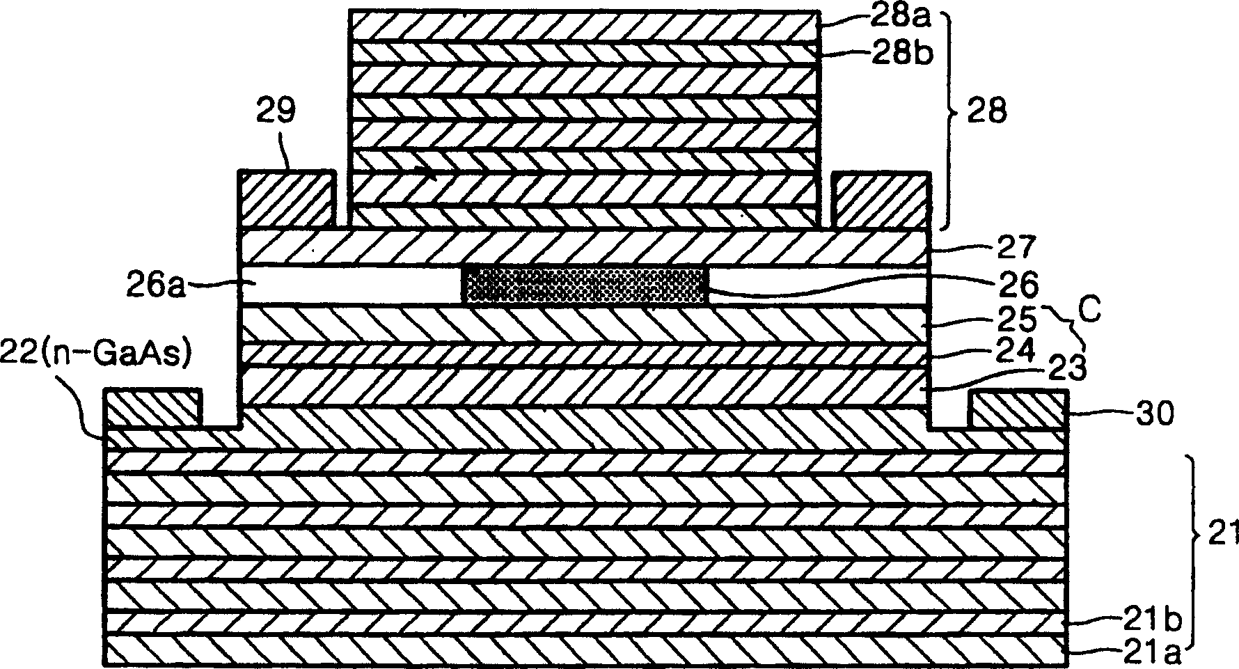
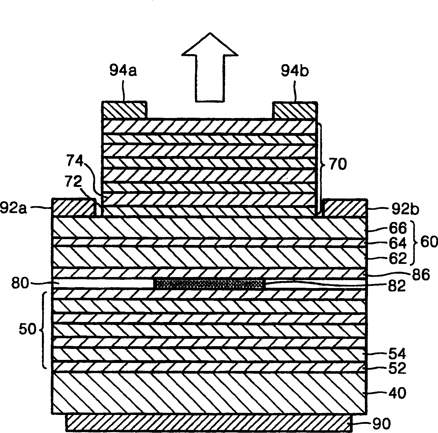
[0018] The wavelength tunable VCSEL in an embodiment of the present invention will be described below with reference to the accompanying drawings. For clarity, the thickness of each layer or each area in the figure has been exaggerated.

[0019] See figure 2 , Reference numeral 40 denotes a substrate, which is a compound semiconductor substrate on which upper and lower distributed Bragg reflectors (DBRs) 50 and 70 and a cavity resonance layer 60 are formed. The lower DBR 50 is formed on the substrate 40. The lower DBR 50 is formed by alternately stacking first and second compound semiconductor layers 52 and 54. The first and second compound semiconductor layers 52 and 54 preferably do not absorb light emitted from the cavity resonance layer 60. Therefore, the energy band gaps of the first and second compound semiconductor layers 52 and 54 are preferably larger than the resonance wavelength. For example, both the first and second compound semiconductor layers 52 and 54 are prefera...


PUM


Abstract

The invention relates to a wavelength-tunable vertical cavity surface-emitting laser diode (VCSEL). The wavelength-tunable VCSEL includes a current-limiting layer formed on a lower distributed Bragg reflector; upper and lower electrodes for laser resonance; and forming An auxiliary electrode on a predetermined area of ​​the upper distributed Bragg reflector from which light is emitted, said auxiliary electrode being used to vary the width of the effective resonance region. Compared with the existing VCSEL, the wavelength tunable VCSEL of the present invention can rapidly change the wavelength of emitted light, and can avoid the deterioration of the laser resonance gain characteristics caused by the change of the width of the effective resonance region due to the temperature change. Therefore, the wavelength tunable region of emitted laser light can be widened.

Description

Technical field [0001] The invention relates to a semiconductor laser, in particular to a wavelength tunable vertical cavity surface emitting laser diode (VCSEL). Background technique [0002] The VCSEL structure has multiple distributed Bragg reflectors (DBRs), each of which has a refractive index of 99%, and they are formed above and below the active layer so as to be in a direction perpendicular to each stack Make the light resonate. The DBR is made by stacking a variety of materials with very different refractive indexes and similar lattice constants to facilitate crystal epitaxial growth, for example: alternately stacking GaAs and AlAs or alternately stacking two dielectric materials with very different refractive indexes Therefore, the two dielectric materials can be obtained from, for example, silicon dioxide SiO 2 Layer, aluminum oxide Al 2 O 3 Layer and titanium oxide TiO 2 Select from the layer. In this DBR, it is better to make the energy band gap larger than the reson...

Claims


Application Information

Patent Timeline
Patent Type & Authority Patents(China)
IPC IPC(8): H01S5/183H01S5/187H01S5/343H01S5/18H01S5/042
CPCB82Y10/00B82Y20/00H01S5/0614H01S5/18311H01S5/18325
Inventor 金泽
Owner SAMSUNG ELECTRONICS CO LTD
Why Eureka
Try Eureka