Liquid crystal display with transparent conductive film on sandwich insulated film formed by coating
A technology of liquid crystal display and transparent conductive film, which is applied in semiconductor/solid-state device manufacturing, instruments, circuits, etc., and can solve the problem of high total resistance
- Summary
- Abstract
- Description
- Claims
- Application Information
AI Technical Summary
Problems solved by technology
Method used
Image
Examples
no. 1 example
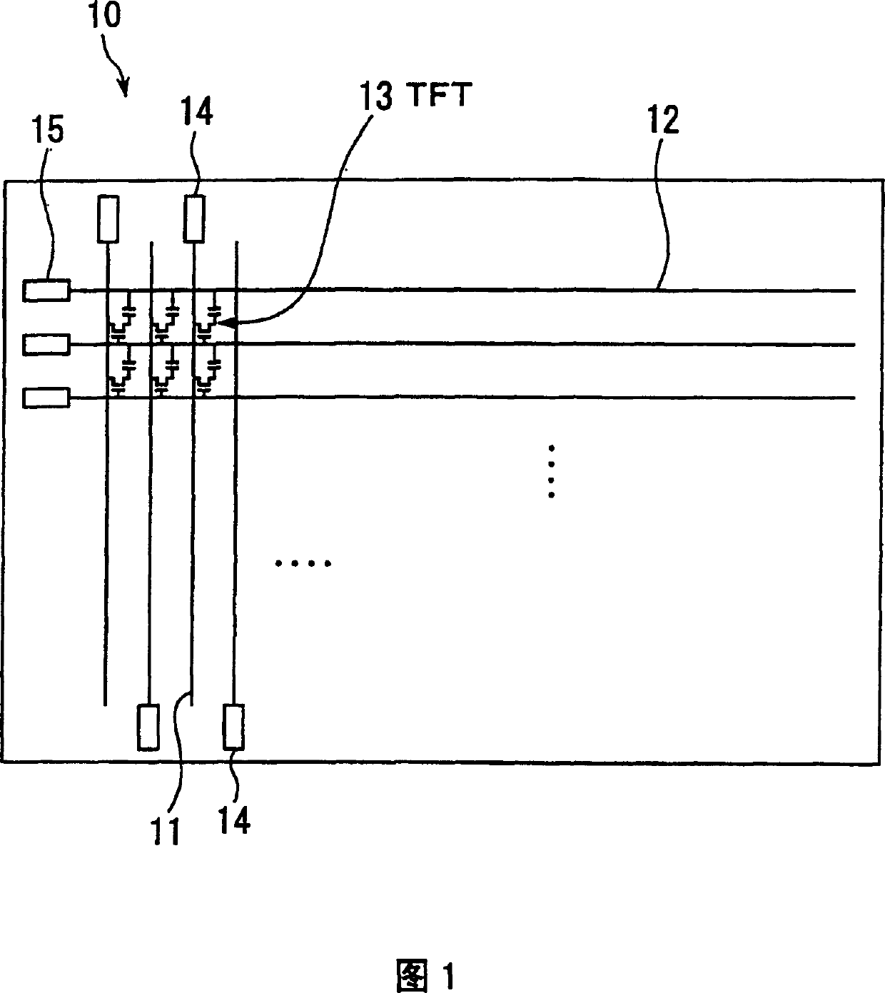
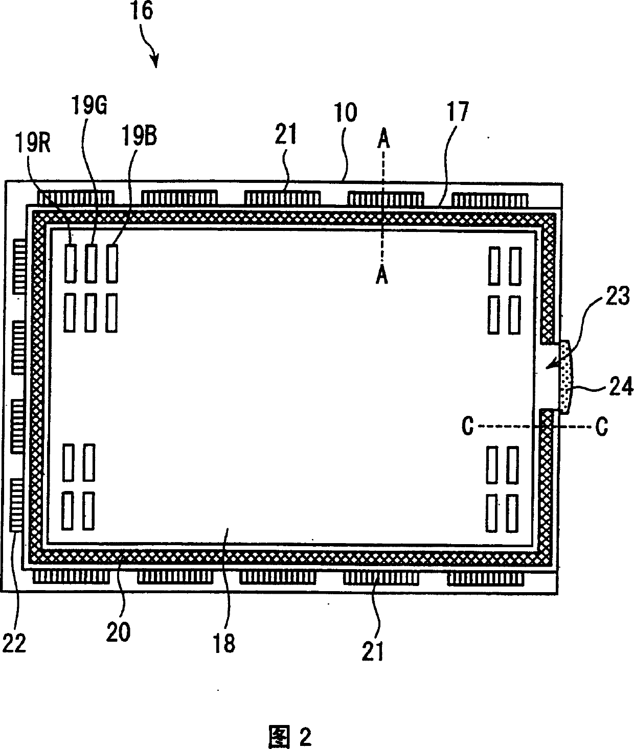
[0070] Fig. 1 is a schematic plan view illustrating the structure of a TFT substrate of a transmissive liquid crystal display according to a first embodiment of the present invention. The TFT substrate 10 shown in FIG. 1 and the opposing substrate 17 mentioned later face each other, and a liquid crystal material is filled in the space between the TFT substrate 10 and the opposing substrate 17 to form a liquid crystal display. The liquid crystal display panel (see Figure 2 and Figure 4).
[0071] On the surface of the TFT substrate 10 facing the opposite substrate 17 side, a plurality of signal lines 11 and a plurality of scanning lines 12 intersecting the signal lines 11 are provided in a grid shape. In the vicinity of each intersection of one of the signal lines 11 and one of the scanning lines 12, a TFT 13 is formed. Therefore, the TFT 13 is arranged in a matrix.
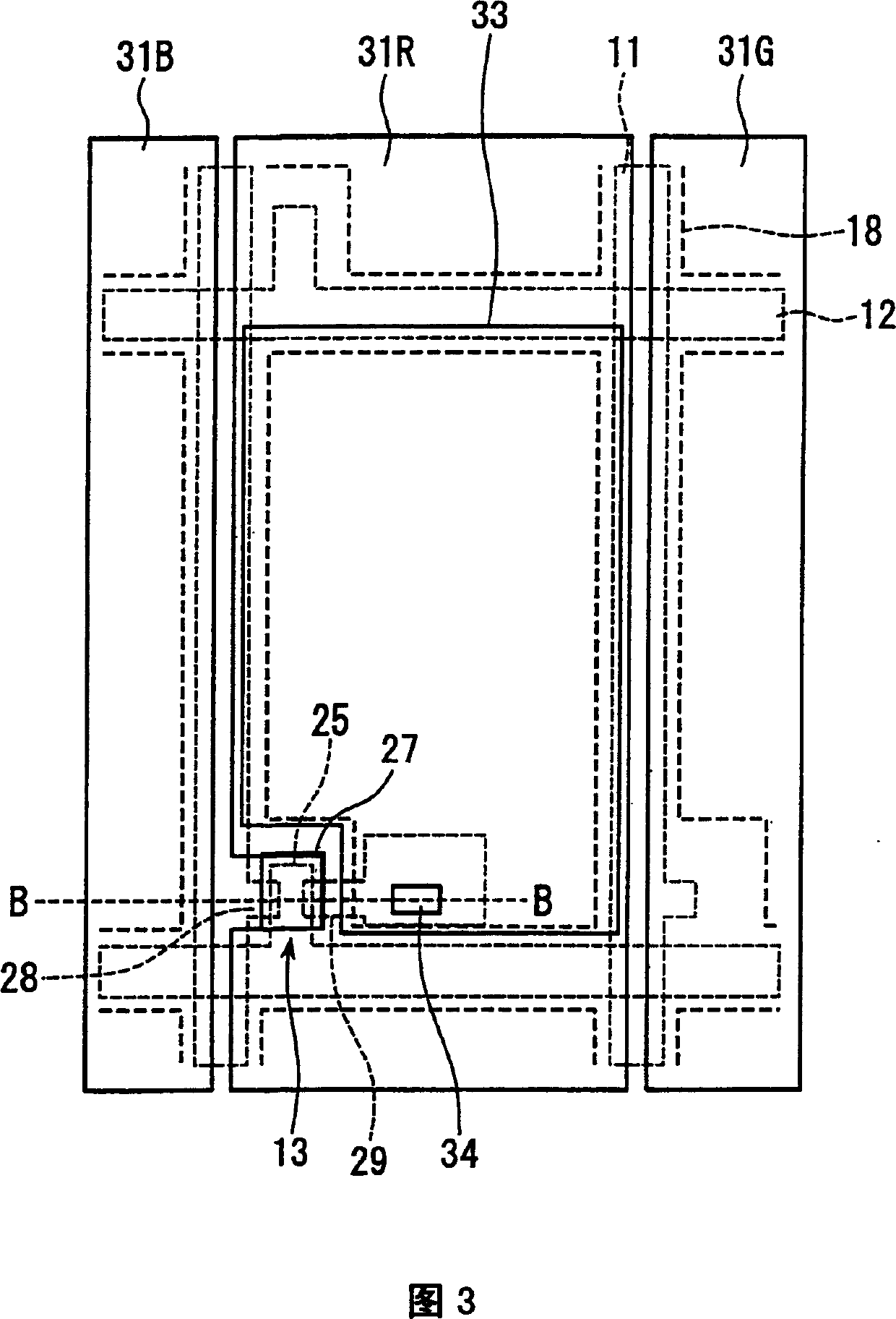
[0072] In this embodiment, the TFT13 constitutes a high-resolution liquid crystal display panel with a CF (color fi...
no. 2 example
[0116] FIG. 10 is a schematic plan view describing the structure of a TFT substrate 50 in a transmissive liquid crystal display according to a second embodiment of the present invention. As shown in FIG. 10, on the surface of the TFT substrate 50 on the opposite substrate side not shown in the drawing, a plurality of signal lines 11 and a plurality of signal lines 11 intersecting with the signal lines 11 are arranged in a grid-like arrangement. Scan line 12. In the vicinity of the intersection of one of the signal lines 11 and one of the scanning lines 12, a TFT 13 is formed. Thus, the TFTs 13 are arranged in a matrix.
[0117] A common wiring conductor, that is, a common wiring 51 is also provided between adjacent scan lines 12. In the common storage type liquid crystal display, the common wiring conductor 51 and the pixel electrode form a storage capacitor.
[0118] The common wiring conductors 51 are coupled to each other, and a common potential is applied thereto. Therefore, c...
PUM
| Property | Measurement | Unit |
|---|---|---|
| temperature | aaaaa | aaaaa |
| thickness | aaaaa | aaaaa |
| thickness | aaaaa | aaaaa |
Abstract
Description
Claims
Application Information
 - R&D
- Intellectual Property
- Life Sciences
- Materials
- Tech Scout
- Unparalleled Data Quality
- Higher Quality Content
- 60% Fewer Hallucinations
Browse by: Latest US Patents, China's latest patents, Technical Efficacy Thesaurus, Application Domain, Technology Topic, Popular Technical Reports.
© 2025 PatSnap. All rights reserved.Legal|Privacy policy|Modern Slavery Act Transparency Statement|Sitemap|About US| Contact US: help@patsnap.com


