Control method, wafer reverse transfer method, post-processing device and wafer processing equipment
A control method and wafer technology, applied in semiconductor/solid-state device manufacturing, electrical components, circuits, etc., can solve problems such as adverse effects of integrated circuit patterns on the wafer surface, residual water film at the stop position of the wafer, and damage to the pattern structure , to achieve the effect of improving the degree of intelligence, realizing wafer protection, and reducing wafer waste
- Summary
- Abstract
- Description
- Claims
- Application Information
AI Technical Summary
Problems solved by technology
Method used
Image
Examples
Embodiment 1
[0065] like Figure 8 As shown, an embodiment of the present invention provides a control method applied to post-processing, including:
[0066] Step S81, after the wafer stops moving due to an abnormality in the wafer cleaning, the wafer position is determined according to the parameters of the actuator; specifically, the current specific movement position of the mechanism can be known according to the motor encoder data of each mechanism, so as to obtain the wafer Location.
[0067] Step S82 , according to different wafer positions, a corresponding abnormal processing prompt is given or wafer reverse transfer, wafer lift or wafer transfer is automatically performed.
[0068] Specifically include:
[0069] 1) If the wafer position is that the wafer has been completely removed from the liquid level, the operator is prompted to directly remove the wafer or automatically perform wafer transfer;
[0070] 2) If the position of the wafer is that the wafer is under the liquid lev...
Embodiment 2
[0074] like Figure 9 As shown, an embodiment of the present invention proposes a wafer reverse transfer method for responding to an abnormal pull-up alarm, including:
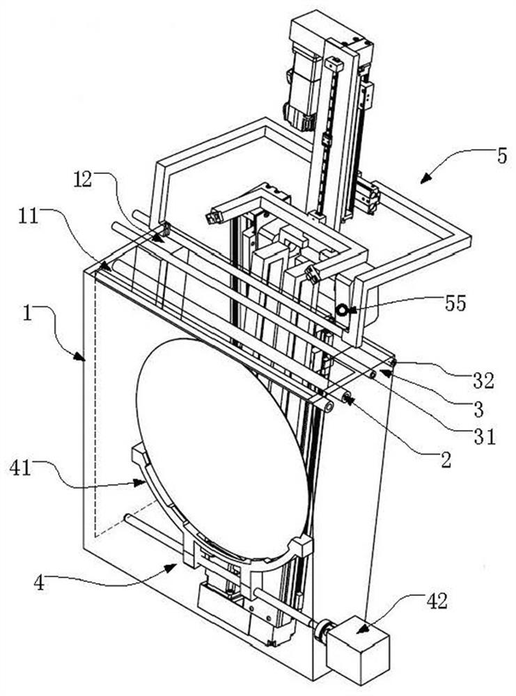
[0075] Step S91, after receiving the reverse transmission instruction, determine the position of the wafer and the state of the mechanism; wherein, the position of the wafer refers to the position of the wafer on the wafer lifting device 5, and can also reflect the lifting mechanism 51, The state of the mechanism of the follower mechanism 52 and the clamping mechanism 53 .
[0076] Specifically, the first in-position sensor 54 and the second in-position sensor 55 are used to detect whether the wafer is in position, and the motor parameters of the lifting mechanism 51 , the follower mechanism 52 and the clamping mechanism 53 are used to determine whether the wafer is in position. the position of the circle.
[0077] Step S92, according to the preset judgment condition and the pre-stored reverse transmission l...
no. 1 Embodiment approach
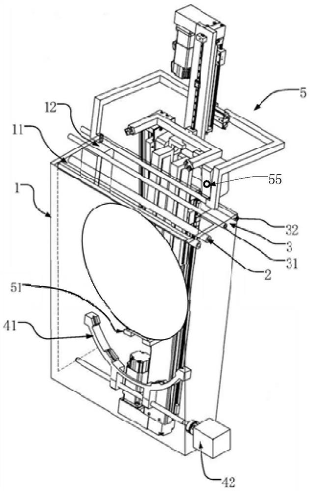
[0084] When the first in-position sensor 54 detects that a wafer is in position, and the second in-position sensor 55 does not detect that a wafer is in position, and the motor motion position parameter of the jacking mechanism 51 is smaller than the first reference point, such as Figure 4 As shown, the first reference point of the motor movement position of the jacking mechanism 51 is the position of the motor of the jacking mechanism 51 when the follower just starts to move, indicating that the wafer is currently only lifted by the jacking mechanism 51, that is image 3 In the state shown in , perform the following operations to perform the reverse transfer:
[0085] Control the lifting mechanism 51 to bring the wafer back to the lowest position;
[0086] After the system returns to normal, perform wafer cleaning and drying again.
PUM
 Abstract
Description
Claims
Application Information
 - R&D
- Intellectual Property
- Life Sciences
- Materials
- Tech Scout
- Unparalleled Data Quality
- Higher Quality Content
- 60% Fewer Hallucinations
Browse by: Latest US Patents, China's latest patents, Technical Efficacy Thesaurus, Application Domain, Technology Topic, Popular Technical Reports.
© 2025 PatSnap. All rights reserved.Legal|Privacy policy|Modern Slavery Act Transparency Statement|Sitemap|About US| Contact US: help@patsnap.com


