Wafer level system packaging method and packaging structure
A system packaging and wafer-level technology, applied in the direction of microstructure technology, microstructure devices, manufacturing microstructure devices, etc., can solve the problems of incompatibility with chip technology and low efficiency of wafer-level system packaging, and achieve high packaging efficiency, The effect of saving process steps and simplifying the process
- Summary
- Abstract
- Description
- Claims
- Application Information
AI Technical Summary
Problems solved by technology
Method used
Image


Examples
Embodiment 1
[0034] The present invention provides a wafer-level system packaging method, comprising:
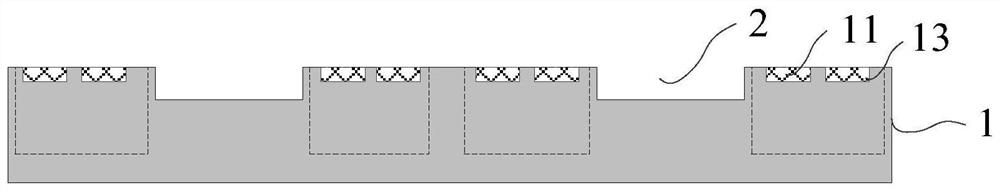
[0035] S01: Provide a device wafer, the surface of the device wafer has a plurality of exposed first bonding pads, a first cavity is formed on the surface of the device wafer, and the first bonding pads are located on the periphery of the first cavity.
[0036] S02: Provide a first chip, where the first chip has a plurality of exposed second pads.
[0037] S03: Bond the first chip to the device wafer, at least part of the first chip is located on the first cavity, the second pad is opposite to the first pad to enclose a first gap, and the first cavity is used as the upper The working chamber of a chip.
[0038] S04: A conductive bump is formed in the first void by an electroplating process, and the conductive bump is electrically connected to the first bonding pad and the second bonding pad.
[0039] It should be noted that S04 in this specification does not represent the order of the ...
Embodiment 2
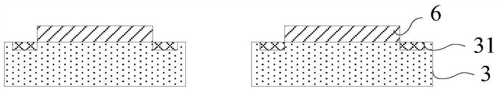
[0084] refer to Figure 14 , and the difference from Embodiment 1 is that the first chip 3 is formed with a second chip 7 , and the second chip 7 is electrically connected to the first chip 3 . In this embodiment, when the first chip is provided, a plurality of exposed third bonding pads are formed on the first chip 3, and the third bonding pads and the second bonding pads 31 are respectively located on both sides of the first chip 3; After the conductive bumps 5, a second chip 7 is provided; the second chip 7 is then bonded to the first chip 3, and a second gap is formed between the second chip 7 and the first chip 3, and is formed in the second gap The conductive block is used to electrically connect the first chip and the second chip. It should be noted that the second chip 7 may only be electrically connected to the first chip 3 , or may be electrically connected to the device wafer 1 through the first chip 3 .
[0085] The bonding of the second chip 7 and the first chip...
Embodiment 3
[0088] refer to Figure 16 , the first chip 3 in Embodiment 1 is bonded to the front side of the device wafer 1. The difference between Embodiment 3 and Embodiment 1 is that the backside of the device wafer 1 is also bonded to the second chip 7, which is connected to the The device wafer 1 is electrically connected. The method for bonding the second chip 7 to the back of the device wafer 1 includes: providing the second chip 7 , and the second chip 7 is bonded to the back of the device wafer 1 . It should be noted that the bonding and electrical connection method between the second chip 7 and the device wafer 1 refer to the bonding and electrical connection method between the first chip 3 and the device wafer 1 in Embodiment 4, which will not be repeated here. In addition, the second chip 7 may be bonded to the device wafer 1 prior to the first chip 3 , or may be bonded to the device wafer 1 after the first chip 3 is bonded to the device wafer 1 .
[0089] When the second ch...
PUM
| Property | Measurement | Unit |
|---|---|---|
| Thickness | aaaaa | aaaaa |
| Thickness | aaaaa | aaaaa |
| Height | aaaaa | aaaaa |
Abstract
Description
Claims
Application Information
 - Generate Ideas
- Intellectual Property
- Life Sciences
- Materials
- Tech Scout
- Unparalleled Data Quality
- Higher Quality Content
- 60% Fewer Hallucinations
Browse by: Latest US Patents, China's latest patents, Technical Efficacy Thesaurus, Application Domain, Technology Topic, Popular Technical Reports.
© 2025 PatSnap. All rights reserved.Legal|Privacy policy|Modern Slavery Act Transparency Statement|Sitemap|About US| Contact US: help@patsnap.com