Package structure and manufacturing method thereof

A packaging structure and manufacturing method technology, applied in the direction of microstructure technology, microstructure devices, manufacturing microstructure devices, etc., can solve the problems of unfavorable packaging structure miniaturization, large area, etc., to achieve miniaturization, increase area, improve Yield and Reliability Effects

Pending Publication Date: 2022-07-08
WINBOND ELECTRONICS CORP
View PDF0 Cites 0 Cited by
  • Summary
  • Abstract
  • Description
  • Claims
  • Application Information

AI Technical Summary

Problems solved by technology

Therefore, the area of ​​the MEMS device is large, which is not conducive to the miniaturization of the packaging structure.

Method used


Image

  • Package structure and manufacturing method thereof
  • Package structure and manufacturing method thereof
  • Package structure and manufacturing method thereof

Examples


Embodiment Construction

[0019] In order to make the above-mentioned and other objects, features and advantages of the present invention more clearly understood, preferred embodiments are given below and described in detail in conjunction with the accompanying drawings. Furthermore, repeated reference symbols and / or wording may be used in different examples of the present invention. These repeated symbols or words are used for the purpose of simplicity and clarity, and are not used to limit the relationship between the various embodiments and / or the described appearance structures.

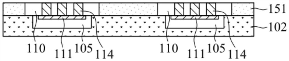
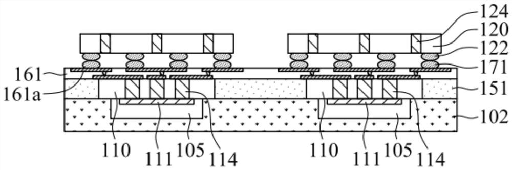
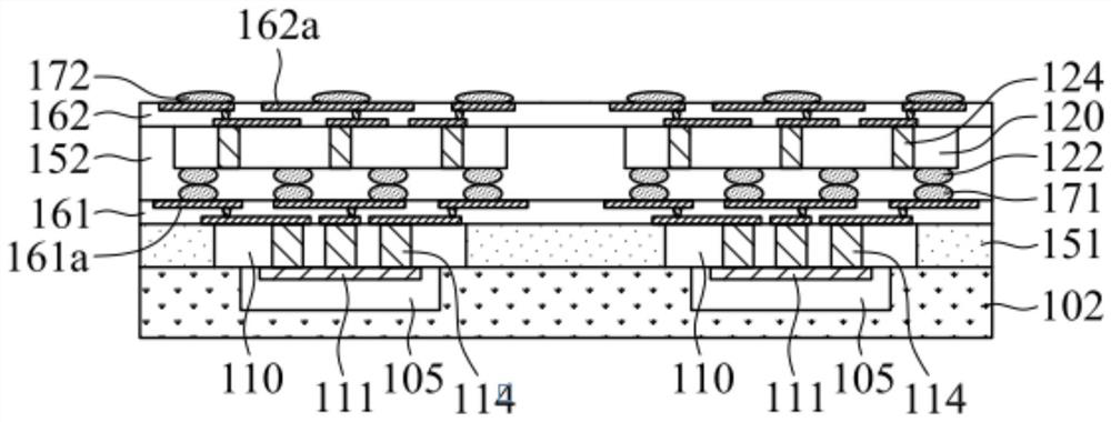
[0020] The present invention provides a package structure and a manufacturing method thereof, Figures 1A to 1F It is a schematic cross-sectional view of the package structure 100 in various stages of the process according to some embodiments of the present invention.

[0021] Please refer to Figure 1A , a substrate 102 having a plurality of notches 105 is provided. Next, corresponding to the positions of these notches...


PUM


Abstract

The invention provides a packaging structure and a manufacturing method thereof. The packaging structure comprises a substrate with a notch, and a first micro-electro-mechanical system chip, a first middle chip, a second micro-electro-mechanical system chip and a first cover plate which are sequentially formed on the substrate. The lower surface of the first micro electro mechanical system chip is provided with a first sensor or a micro actuator. The upper surface of the second micro electro mechanical system chip is provided with a second sensor or a micro actuator. The first middle chip is provided with a substrate through hole and comprises a signal conversion unit, a logic operation unit, a control unit or a combination of the signal conversion unit, the logic operation unit and the control unit. The package structure includes at least one of a first sensor and a second sensor.

Description

technical field [0001] The present invention relates to a package structure, and more particularly, to a package structure with a three-dimensional MEMS chip stack and a method for manufacturing the same. Background technique [0002] Microelectromechanical system (microelectromechanical system, MEMS) is a technology that combines microelectronics technology and mechanical engineering. MEMS technology enables the miniaturization of many industrial devices. The MEMS device usually includes a microprocessor and at least one miniature sensor for obtaining external information. [0003] For current MEMS devices, it is usually necessary to assemble multiple MEMS elements in the same package structure, and to integrate the operations of these MEMS elements. However, if the two MEMS elements are too close, their signals may interfere with each other. As a result, the yield and reliability of the MEMS device will be reduced. [0004] On the other hand, in the packaging structure...

Claims


Application Information

Patent Timeline
IPC IPC(8): B81B7/00B81B7/02B81C1/00
CPCB81B7/0074B81B7/0064B81B7/02B81C1/00333
Inventor 吴金能
Owner WINBOND ELECTRONICS CORP
Why Eureka
Try Eureka