Bonding packaging structure of diode and process thereof

A packaging structure, diode technology, applied in the direction of semiconductor/solid-state device parts, semiconductor devices, electrical components, etc., can solve the problems of uneven current flow, low chip bonding reliability, mismatching thermal expansion coefficient, etc., and achieve electrical performance Normal, guaranteed long-term reliability, suitable for soldering effect

Pending Publication Date: 2022-05-13
济南市半导体元件实验所
View PDF0 Cites 0 Cited by
  • Summary
  • Abstract
  • Description
  • Claims
  • Application Information

AI Technical Summary

Problems solved by technology

[0004] In order to solve the above problems, the present invention proposes a diode bonding package structure and its technology, changing the metal layer on the chip surface, adding a molybdenum sheet as a transition piece, and solving the problem of low chip bonding reliability and low thermal expansion coefficient in the prior art. Matching, current uneven current and other problems, improve the long-term reliability of the product

Method used


Image

  • Bonding packaging structure of diode and process thereof
  • Bonding packaging structure of diode and process thereof
  • Bonding packaging structure of diode and process thereof

Examples


Embodiment 2

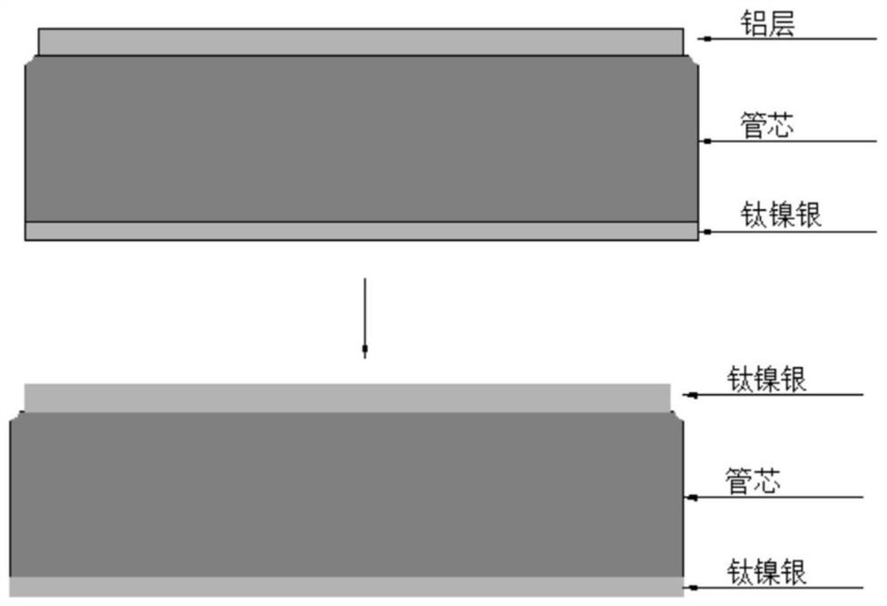
[0056] This embodiment provides a bonding packaging process for the bonding packaging structure of the diode described in Embodiment +, including:

[0057] Metallize the chip with titanium-nickel-silver;

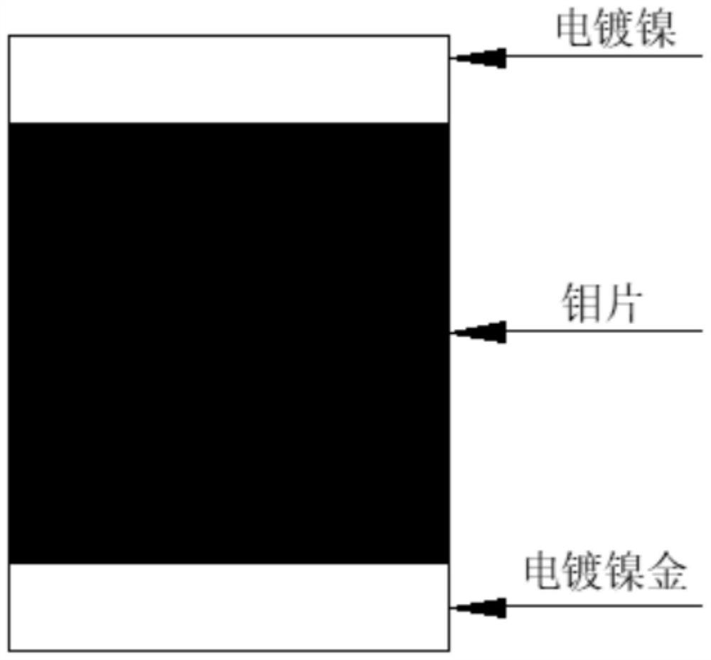
[0058] Metallization of the welding surface and the bonding surface of the molybdenum sheet, wherein the welding surface of the molybdenum sheet is electroplated with nickel gold, and the bonding surface of the molybdenum sheet is electroplated with nickel;

[0059] Vacuum welding the welding surface of the molybdenum sheet and the chip;

[0060] Ultrasonic bonding is performed on the bonding surface of the molybdenum sheet and the bonding wire.

[0061] This embodiment adopts the vacuum welding transition piece process to ensure the bonding quality. The process of metallizing titanium nickel silver is carried out on the chip surface, and the transition piece is vacuum welded on the chip surface. The welding and bonding process of the transition piece not only ensures the b...


PUM


Abstract

The invention discloses a bonding packaging structure of a diode and a process thereof. The bonding packaging structure comprises a chip, a molybdenum sheet and a bonding wire, titanium-nickel-silver metallization is carried out on the chip, nickel-gold is electroplated on one side of the molybdenum sheet, nickel is electroplated on the other side of the molybdenum sheet, the nickel-gold electroplated side of the molybdenum sheet is welded on the chip, and the nickel-plated side of the molybdenum sheet is ultrasonically bonded with the bonding wire. A metal layer on the surface of the chip is changed, and a molybdenum sheet is added as a transition sheet, so that the problems of low chip bonding reliability, mismatched thermal expansion coefficients, non-uniform current and the like in the prior art are solved, and the long-term reliability of a product is improved.

Description

technical field [0001] The invention relates to the technical field of diode bonding and packaging, in particular to a diode bonding and packaging structure and a process thereof. Background technique [0002] The statements in this section merely provide background information related to the present invention and do not necessarily constitute prior art. [0003] Due to the low cost of the wafer of the diffuser, easy production, and mature technology, the production of high-power diode wafers mostly adopts the diffuser process; however, after the sandblasting process of the diffuser, the surface of the wafer has Related to) unevenness, in the subsequent chip bonding and packaging process, due to the micro-defects on the surface, after ultrasonic bonding, the bonding quality decays rapidly after 500 temperature cycles (-55℃~++50℃). There is a problem of long-term reliability of the bonding process; and due to the large current, there is a problem of uneven chip current flow....

Claims


Application Information

Patent Timeline
Patent Type & Authority Applications(China)
IPC IPC(8): H01L23/492H01L21/60
CPCH01L23/4924H01L24/83H01L2224/83H01L2924/01042H01L2224/49111H01L2224/48247
Inventor 王迎春薄霞马捷杨敏
Owner 济南市半导体元件实验所
Why Eureka
Try Eureka