LED packaging method and LED lamp

A technology of LED packaging and LED lights, which is applied in the direction of electrical components, circuits, semiconductor devices, etc., can solve problems such as color coordinate drift, and achieve the effects of reducing heat, avoiding color coordinate drift, and avoiding luminous flux reduction

Pending Publication Date: 2022-03-25
SHENZHEN RUNLITE TECH
View PDF0 Cites 0 Cited by
  • Summary
  • Abstract
  • Description
  • Claims
  • Application Information

AI Technical Summary

Problems solved by technology

[0003] The technical problem to be solved by the present invention is to provide an LED packaging method and an LED lamp to solve the problem of how to avoid color coordinate drift while reducing the temperature of the LED chip

Method used


Image

  • LED packaging method and LED lamp
  • LED packaging method and LED lamp
  • LED packaging method and LED lamp

Examples


Embodiment 1

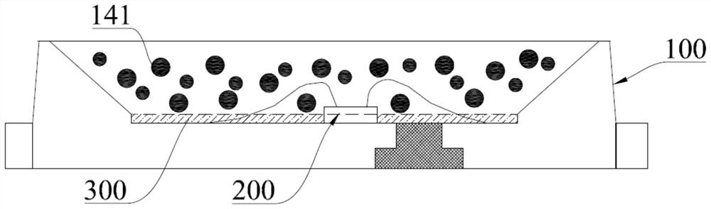
[0050] Please refer to Figure 5 and Figure 13 to Figure 16 , Embodiment 1 of the present invention is: an LED packaging method, which is applied to the production process of LED lamps and LED modules.

[0051] Described LED packaging method comprises the steps:

[0052] S11, providing a bracket 100 and at least one LED chip 200;

[0053] S12, fixing the LED chip 200 on the support 100 through the thermally conductive adhesive layer 110;

[0054] S13, performing wire bonding on the LED chip 200 and the bracket 100;

[0055] S14, setting the first silica gel layer 130 covering the LED chip 200 on the bracket 100;

[0056] S15 , disposing a second silica gel layer 140 mixed with fluorescent powder 141 on the first silica gel layer 130 .

[0057] The working principle of the LED packaging method in this embodiment is as follows: the LED chip 200 is fixed on the bracket 100 through the thermally conductive adhesive layer 110, and conducts heat to the bracket 100 when the LED...

Embodiment 2

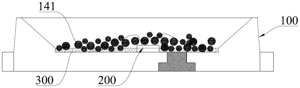
[0061] refer to Figure 6 to Figure 16 , Embodiment 2 of the present invention provides another specific implementation of the LED packaging method.

[0062] Described LED packaging method comprises the steps:

[0063] S20, providing a bracket 100 and at least one LED chip 200;

[0064] S21, fixing the LED chip 200 on the bracket 100 through the thermally conductive adhesive layer 110;

[0065] S22 , fixing the edge of the LED chip 200 on the bracket 100 through the transparent glue layer 120 .

[0066] S23, performing wire bonding on the LED chip 200 and the bracket 100;

[0067] S24, setting the first silica gel layer 130 covering the LED chip 200 on the bracket 100;

[0068] S25 , disposing a second silica gel layer 140 mixed with fluorescent powder 141 on the first silica gel layer 130 .

[0069] The working principle of the LED packaging method in this embodiment is as follows: the LED chip 200 is fixed on the bracket 100 through the thermally conductive adhesive lay...


PUM

PropertyMeasurementUnit
thicknessaaaaaaaaaa
thermal conductivityaaaaaaaaaa

Abstract

The invention discloses an LED packaging method and an LED lamp. The method comprises the following steps: providing a bracket and at least one LED chip; fixing the LED chip on the bracket through a heat-conducting glue layer; carrying out wire bonding treatment on the LED chip and the bracket; a first silica gel layer covering the LED chip is arranged on the support; and a second silica gel layer mixed with fluorescent powder is arranged on the first silica gel layer. The LED chip is fixed on the support through the heat-conducting glue layer, so that light emitted by the LED chip can be effectively conducted to the support, heat of the LED chip is reduced, and luminous flux emitted by the LED chip is prevented from being reduced. Meanwhile, the LED chip and the fluorescent powder are separated by arranging the first silica gel layer, the excitation effect of the fluorescent powder is prevented from being affected by heating of the LED chip, and therefore the problem of color coordinate drifting is avoided.

Description

technical field [0001] The invention relates to the technical field of LED packaging, in particular to an LED packaging process and an LED lamp. Background technique [0002] LED (Light-Emitting Diode, light-emitting diode) is a commonly used light-emitting device. The common LED production process is to set the LED chip on the bracket, and then perform the steps of solid crystal, wire bonding, powder application and baking in sequence. Because the temperature rise of the LED chip when it emits light will cause the brightness to decrease, the current production process is through the phosphor deposition process, which uses the phosphor deposition to attach to the LED chip and the bottom of the bracket, and conducts the heat of the LED chip to the bracket, but the LED chip produces The transfer of heat to the phosphor will make the excitation effect of the phosphor worse after being heated, resulting in the phenomenon of color coordinate drift. Contents of the invention ...

Claims


Application Information

Patent Timeline
Patent Type & Authority Applications(China)
IPC IPC(8): H01L33/00H01L33/52H01L33/64
CPCH01L33/005H01L33/52H01L33/641H01L2933/005H01L2933/0075
Inventor 周文叶仕安熊章丽
Owner SHENZHEN RUNLITE TECH
Why Eureka
Try Eureka