
Pixel unit with driving IC, light-emitting device comprising pixel unit and manufacturing method thereof

A light-emitting device and pixel unit technology, which is applied in the fields of electrical components, semiconductor/solid-state device manufacturing, and instruments, can solve the problems of high cost of control circuits and increased costs, and achieve low production costs, high integration, and good mass production rate Effect

Pending Publication Date: 2022-03-11
INNOSERV +1
View PDF0 Cites 1 Cited by
  • Summary
  • Abstract
  • Description
  • Claims
  • Application Information

AI Technical Summary

Problems solved by technology

Therefore, the cost of control circuits manufactured according to TFT technology is very expensive
At the same time, the production of large-scale active arrays by TFT technology requires large-area deposition of thin-film machines or equipment, which substantially increases the cost of manufacturing and becomes the threshold for a small number of investors to operate high-cost TFT technology.

Method used


Image

  • Pixel unit with driving IC, light-emitting device comprising pixel unit and manufacturing method thereof
  • Pixel unit with driving IC, light-emitting device comprising pixel unit and manufacturing method thereof
  • Pixel unit with driving IC, light-emitting device comprising pixel unit and manufacturing method thereof

Examples


Embodiment Construction

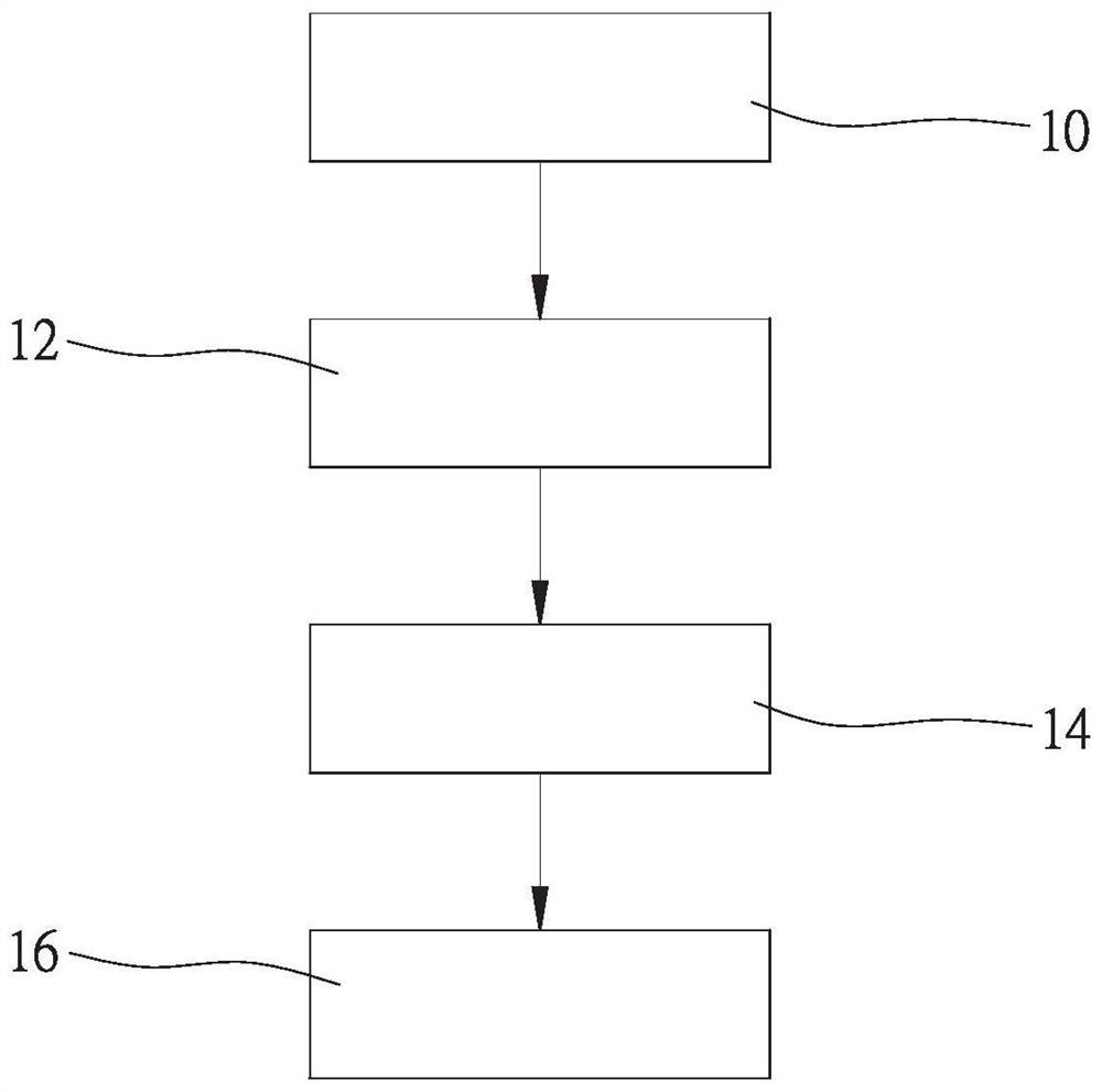
[0033] figure 1 It is a flow chart. Step 10, step 2 12, step 3 14 to step 4 16 are executed to manufacture a light-emitting device in the present invention.

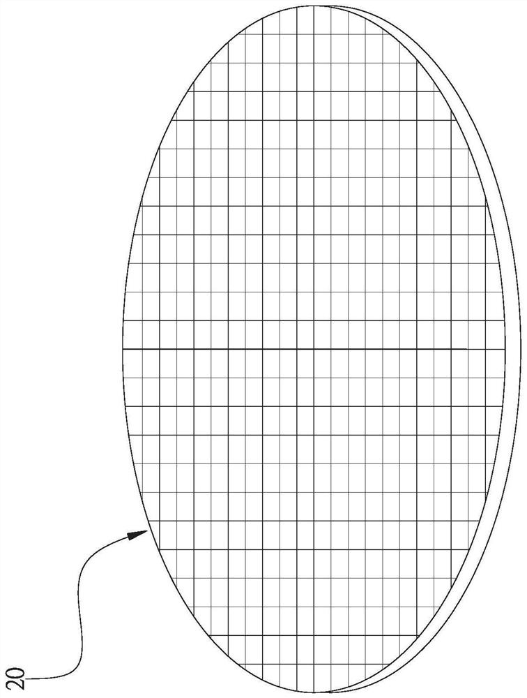
[0034] Wherein, step 10 refers to: a driver integrated circuit wafer is equipped with multiple control circuits.

[0035] Step 2 12 refers to three micro-LEDs that emit red, green and blue light as a group when electrified, multiple groups of micro-LEDs are stacked on the driver integrated circuit wafer, and are electrically connected to the corresponding control circuit for packaging.

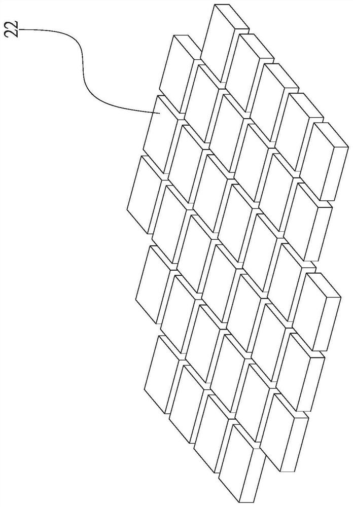
[0036] Step 3 14 refers to: the packaged driver IC wafer is laser cut into multiple driver ICs, and the control circuit of the driver ICs is electrically connected to a single group of micro LEDs to form a pixel unit in a 3D package stack structure.

[0037] As for step 4 16: multiple pixel units are transferred to the electronic circuits of the single display substrate to be connected in series to form a single-chip light emitting devi...


PUM

PropertyMeasurementUnit
sizeaaaaaaaaaa
thicknessaaaaaaaaaa
sizeaaaaaaaaaa

Abstract

The invention discloses a manufacturing method of a light-emitting device, a pixel unit and the light-emitting device. The manufacturing method of the light-emitting device comprises the steps that a driving integrated circuit wafer is provided with a plurality of control circuits; three miniature LEDs which emit red light, green light and blue light after being electrified form a group, and a plurality of groups of miniature LEDs are stacked on a driving integrated circuit wafer and are electrically connected with corresponding control circuits to be packaged. The packaged driving integrated circuit wafer is cut into a plurality of driving ICs through laser, and a control circuit of each driving IC is electrically connected with a single group of miniature LEDs to form a pixel unit of a 3D packaging stack structure; and the electronic circuits, transferred to the single-chip display substrates, of the pixel units are connected in series and combined into a single-chip light-emitting device, and the electronic circuits electrically connected with the display substrates form a multi-chip light-emitting device. Therefore, the pixel unit with the driving IC can be manufactured, the occupied surface area of the display substrate is minimum, the excellent filling rate is provided, the advantage of maximizing the transparent area is achieved, and the pixel unit becomes an ideal choice of a transparent display.

Description

technical field [0001] The present invention relates to the technical field of displays, in particular to a pixel unit, which itself has a driver IC; a light emitting device including the pixel unit; and a manufacturing method, a process for producing the pixel unit and the light emitting device. Background technique [0002] Known displays include a plurality of light emitting elements or pixels controlled by an array of circuits (or active array). The circuit array includes one or more transistors to drive the associated pixels; and one or more capacitors are used to maintain the pixel bias for multiple updates of the display. [0003] So far, through liquid crystal technology (ie, liquid crystal display panel, abbreviated as LCD) and plasma technology (ie, plasma display panel), the display has a light-emitting panel with a large size and a long service life. However, liquid crystal display panels have problems such as power efficiency and directivity, while plasma displ...

Claims


Application Information

Patent Timeline
Patent Type & Authority Applications(China)
IPC IPC(8): H01L27/15H01L33/48H01L33/62H01L21/78G09G3/32
CPCH01L27/156H01L33/48H01L33/62H01L21/78G09G3/32H01L2933/0033H01L2933/0066
Inventor 吴智孟田建国林俊忠
Owner INNOSERV
Learn More