High-brightness high-power semiconductor light-emitting device and preparation method thereof
A technology of light-emitting devices and semiconductors, applied in the direction of semiconductor lasers, laser components, optical waveguide semiconductor structures, etc., can solve the problems of high reliability, low cost, high integration, etc., to achieve reduced divergence angle, small divergence, light Divergent large effect
- Summary
- Abstract
- Description
- Claims
- Application Information
AI Technical Summary
Problems solved by technology
Method used
Image

Examples
Embodiment 1
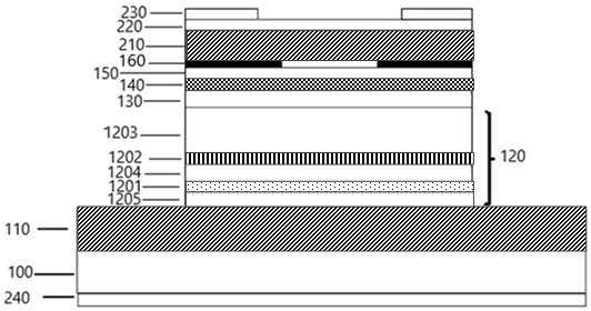
[0032]An embodiment of the present invention provides a high-brightness high-power semiconductor light-emitting device, refer to figure 1 ,include:
[0033] Semiconductor substrate layer 100;
[0034] A modulation structure 120 located on the semiconductor substrate layer, the modulation structure 120 comprising: a carrier modulation active layer 1201; a modulation structure located on the side of the carrier modulation active layer 1201 away from the semiconductor substrate layer 100 a tunnel junction 1202; a cavity extension layer 1203 located on the side of the modulation tunnel junction 1202 away from the carrier modulation active layer 1201;
[0035] The first active layer 140 located on the side of the modulation structure 120 away from the semiconductor substrate layer 100, the carrier concentration in the carrier modulation active layer 1201 is smaller than that in the first active layer 140 Carrier concentration: the first current confinement layer 160 located on th...
Embodiment 2
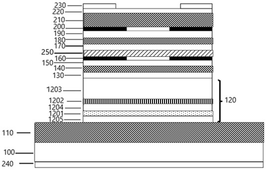
[0055] The difference between this embodiment and embodiment 1 is: refer to figure 2 , between the modulation structure 120 and the second Bragg mirror 210, the first active layer 140 to the Qth active layer are arranged, and Q is an integer greater than or equal to 2; the k+1th active layer is located in the kth active layer On the side away from the modulation structure 120, k is an integer greater than or equal to 1 and less than or equal to Q-1; the high-brightness and high-power semiconductor light-emitting device further includes: a first tunnel junction 250 to a Q-1 tunnel junction , the kth tunnel junction is located between the k+1th active layer and the kth active layer; the first current confinement layer 160 is located between the first tunnel junction 250 and the first active layer 140 .
[0056] The high-brightness and high-power semiconductor light-emitting device of this embodiment further includes: a first Bragg reflector 110 and a second Bragg reflector 210 ...
Embodiment 3
[0065] This embodiment provides a method for preparing a high-brightness and high-power semiconductor light-emitting device. Refer to figure 1 ,include:
[0066] S1: providing a semiconductor substrate layer 100;
[0067] S2: Forming a modulation structure 120 on the semiconductor substrate layer 100, the step of forming the modulation structure 120 includes: forming a carrier modulation active layer 1201 on the semiconductor substrate layer 100; A modulation tunnel junction 1202 is formed on the side of the active layer 1201 away from the semiconductor substrate layer 100; a cavity extension layer 1203 is formed on the side of the modulation tunnel junction 1202 away from the carrier modulation active layer 1201;
[0068] S3: Form the first active layer 140 on the side of the modulation structure 120 away from the semiconductor substrate layer 100, the carrier concentration in the carrier modulation active layer 1201 is smaller than that of the first active layer Carrier co...
PUM
| Property | Measurement | Unit |
|---|---|---|
| thickness | aaaaa | aaaaa |
Abstract
Description
Claims
Application Information
 - R&D
- Intellectual Property
- Life Sciences
- Materials
- Tech Scout
- Unparalleled Data Quality
- Higher Quality Content
- 60% Fewer Hallucinations
Browse by: Latest US Patents, China's latest patents, Technical Efficacy Thesaurus, Application Domain, Technology Topic, Popular Technical Reports.
© 2025 PatSnap. All rights reserved.Legal|Privacy policy|Modern Slavery Act Transparency Statement|Sitemap|About US| Contact US: help@patsnap.com