


Quick Research
Generate reliable direction feasibility study reports for your R&D in just a few steps.

Technical Q&A
Discover and master advanced knowledge NOW. Basics, ideas, possibilities, all at once.

Find Solutions
As an expert in R&D theories, this can generate solutions to your technical problems instantly.

Evaluate Feasibility
Analyze your overall solution with one click, know your potential R&D risks in advance.

Monitor Landscape
Get weekly tech updates, stay abreast of the latest tech innovations and key insights.
Grinding process for polycrystalline silicon layer and wafer
A grinding process, polysilicon layer technology, applied in electrical components, semiconductor/solid-state device manufacturing, circuits, etc., can solve problems such as affecting wafer quality
- Summary
- Abstract
- Description
- Claims
- Application Information
AI Technical Summary
Problems solved by technology
Method used
Image

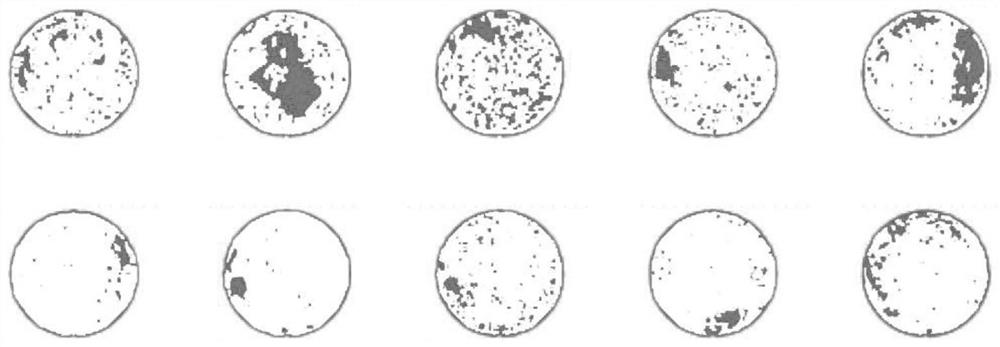
Examples
Embodiment Construction
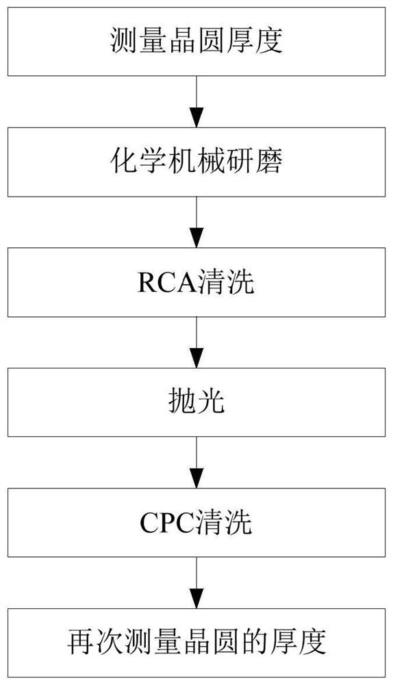
[0022] In order to make the object, technical solution and advantages of the present invention clearer, the present invention will be further described in detail below in conjunction with the embodiments. It should be understood that the specific embodiments described here are only used to explain the present invention, not to limit the present invention.
[0023] figure 2 A specific flow of an embodiment of a polishing process for a polysilicon layer according to the present invention is shown. The grinding process generally includes the following steps:
[0024] 1) Measuring wafer thickness
[0025] Obtain the initial thickness D0 of the wafer before grinding.
[0026] 2) Chemical-mechanical polishing of the polysilicon layer of the wafer to obtain a polished surface
[0027] Abraded surfaces with a certain degree of flatness are obtained based on chemical etching and mechanical removal. In this step, technicians can adjust specific grinding parameters according to dif...
PUM
| Property | Measurement | Unit |
|---|---|---|
| Hardness | aaaaa | aaaaa |
Abstract
Description
Claims
Application Information
 - R&D Engineer
- R&D Manager
- IP Professional
- Industry Leading Data Capabilities
- Powerful AI technology
- Patent DNA Extraction
Browse by: Latest US Patents, China's latest patents, Technical Efficacy Thesaurus, Application Domain, Technology Topic, Popular Technical Reports.
© 2024 PatSnap. All rights reserved.Legal|Privacy policy|Modern Slavery Act Transparency Statement|Sitemap|About US| Contact US: help@patsnap.com