Airtight packaging structure and method for microwave and millimeter wave chip with BGA interface

A hermetic packaging, millimeter wave technology, applied in electrical components, semiconductor/solid-state device parts, semiconductor devices, etc., can solve the problems of increasing link loss, difficulty in repairing, affecting product size, etc., and reducing link Loss, improve service life and reliability, convenient and efficient production

Active Publication Date: 2022-02-25
成都雷电微力科技股份有限公司
View PDF4 Cites 0 Cited by
  • Summary
  • Abstract
  • Description
  • Claims
  • Application Information

AI Technical Summary

Problems solved by technology

This integrated TR module design method is intuitive and highly flexible, but there are many disadvantages, such as: First, external RF connectors and low-frequency connectors are used more, and the cost of connectors and welding processes increase the cost of the product , which increases the difficulty of the process and increases the volume and weight of the product; and for millimeter waves, the introduction of connectors will increase the loss of the link; second, the cavity size of the integrated TR module is generally large, which affects the sealing process The requirements are high, and the cover plate is prone to bulges or depressions, which will affect the external dimensions of the product; and according to theoretical research and engineering experience, under the same process conditions, the larger the cavity, the worse the airtightness; third, due to the module-level packaging, The manufacturing process is complicated, repairing is difficult, and a slight link in the production process is not well controlled, which will result in a decline in the yield rate, which is not suitable for mass production; Modular design ideas will affect the iterative cycle of the project
[0004] Therefore, there is still room for improvement in the existing chip packaging structure and technology. Today's high performance, miniaturization and low cost are urgent needs of the market, so it is necessary to propose a more reasonable and effective method to solve the problems in the existing technology. existing problems

Method used


Image

  • Airtight packaging structure and method for microwave and millimeter wave chip with BGA interface
  • Airtight packaging structure and method for microwave and millimeter wave chip with BGA interface
  • Airtight packaging structure and method for microwave and millimeter wave chip with BGA interface

Examples


Embodiment 1

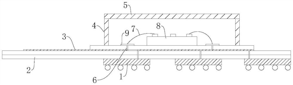
[0042] like figure 1 As shown, a microwave and millimeter wave chip hermetic packaging structure with a BGA interface includes a substrate BGA ball planting array structure 1, and an airtight substrate 2 composed of several layers of circuit substrates is arranged on the substrate BGA ball planting array structure 1. The upper surface of the airtight substrate 2 is provided with a chip assembly 8, and the substrate BGA ball planting array structure 1 passes through the airtight substrate 2 and is communicatively connected with the chip assembly 8; the airtight substrate 2 is provided with a surrounding frame 4 around the chip assembly 8. An airtight cover plate 5 is arranged on the frame 4 to form an airtight chamber for accommodating the chip assembly 8; an antenna radiator 3 is arranged on the airtight substrate 2, and a bonding end 9 is arranged on the airtight substrate 2 in the airtight chamber, The antenna radiator 3 passes through the airtight substrate 2 and is connect...

Embodiment 2

[0055] The content of the above-mentioned embodiment 1 describes a microwave and millimeter-wave chip hermetic packaging structure provided with a BGA interface. This embodiment also discloses other feasible packaging structure solutions, which are now described.

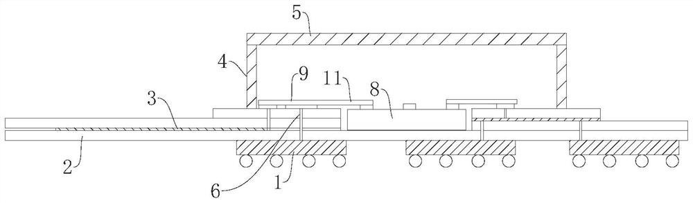
[0056] In this embodiment, the setting structure of the chip assembly 8 is optimized, as follows:

[0057] like Figure 4 As shown, the upper surface of the airtight substrate 2 is provided with a chip BGA ball planting array structure 10, and the bonding end of the chip assembly 8 is bonded and connected to the chip BGA ball planting array structure 10; the chip BGA ball planting array The structure 10 is communicatively connected with the substrate BGA ball planting array structure 1 by passing through the airtight substrate. When such a solution is adopted, the chip components are set up in reverse, and the chip BGA ball planting array structure is connected to the airtight substrate and communicates with the su...

Embodiment 3

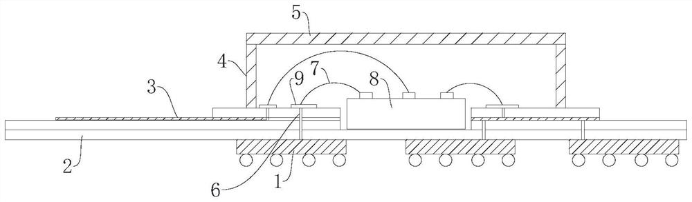
[0062] The content of the above-mentioned embodiment 1 describes a microwave and millimeter-wave chip hermetic packaging structure provided with a BGA interface. This embodiment also discloses other feasible packaging structure solutions, which are now described.

[0063] This embodiment optimizes and improves the settings of the chip components, specifically:

[0064] like figure 2 and image 3 As shown, a microwave and millimeter wave chip hermetic packaging structure with a BGA interface includes a substrate BGA ball planting array structure 1, and an airtight substrate 2 composed of several layers of circuit substrates is arranged on the substrate BGA ball planting array structure 1. The dense substrate 2 is provided with a groove for setting the chip component 8, the chip component 8 is arranged in the groove and bonded with the substrate BGA ball planting array structure 1; the airtight substrate 2 is provided with a surrounding frame 4 around the chip component 8, and...


PUM


Abstract

The invention relates to the technical field of chip packaging, in particular to an airtight packaging structure and method for a microwave and millimeter wave chip with a BGA interface, and the structure comprises a substrate BGA ball mounting array structure, wherein an airtight substrate is arranged on the substrate BGA ball mounting array structure, a chip assembly is arranged on the upper surface of the airtight substrate, and the substrate BGA ball mounting array structure penetrates through the airtight substrate and is in communication connection with the chip assembly; a surrounding frame is arranged on the airtight substrate around the chip assembly, and an airtight cover plate is arranged on the surrounding frame to form an airtight cavity; an antenna radiation part is arranged on the airtight substrate, a bonding end is arranged on the airtight substrate in the airtight cavity, the antenna radiation part penetrates through the airtight substrate and is connected with the bonding end, and the chip assembly is in communication connection with the antenna radiation part through the bonding end. According to the invention, the chip assembly is connected with the antenna radiation part through the bonding end, and there is no need to arrange a connector or an adapter outside the airtight cavity, thereby greatly reducing the link loss, the size and cost of the packaging structure, enabling the production and manufacturing to be more convenient and efficient, and improving the service life and reliability of the packaging structure.

Description

technical field [0001] The invention relates to the technical field of chip packaging, in particular to a microwave and millimeter wave chip hermetic packaging structure and method provided with a BGA interface. Background technique [0002] Hermetic packaging of chips can greatly improve the service life and long-term reliability of microwave and millimeter wave circuits, while an excellent chip packaging solution needs to simultaneously improve product performance, manufacturability, miniaturization, and cost reduction. [0003] At present, the most widely used packaging method in the industry is to solder or bond the microwave and millimeter wave bare chip to the microwave and millimeter wave circuit, and then weld or bond the microwave and millimeter wave circuit board in the metal cavity. The high and low frequency connectors and the outside of the module realize the interconnection of radio frequency signals, control signals and power supply, and use the sealing and we...

Claims


Application Information

Patent Timeline
Patent Type & Authority Applications(China)
IPC IPC(8): H01L23/04H01L23/10H01L23/14H01L23/498H01L23/66
CPCH01L23/04H01L23/10H01L23/14H01L23/49816H01L23/66H01L2223/6677H01L2224/16225H01L2224/48091H01L2924/16152H01L2224/73253H01L2924/00014
Inventor 丁卓富李雪慧陈冲王震
Owner 成都雷电微力科技股份有限公司
Why Eureka
Try Eureka