


Quick Research
Generate reliable direction feasibility study reports for your R&D in just a few steps.

Technical Q&A
Discover and master advanced knowledge NOW. Basics, ideas, possibilities, all at once.

Find Solutions
As an expert in R&D theories, this can generate solutions to your technical problems instantly.

Evaluate Feasibility
Analyze your overall solution with one click, know your potential R&D risks in advance.

Monitor Landscape
Get weekly tech updates, stay abreast of the latest tech innovations and key insights.
Wafer multilayer stacking bonding method
A multi-layer stacking and wafer technology, applied in the manufacturing of electrical components, electric solid-state devices, semiconductor/solid-state devices, etc., can solve problems such as wafer fragments, avoid splits, have broad application prospects and market potential, and improve assembly efficiency Effect
- Summary
- Abstract
- Description
- Claims
- Application Information
AI Technical Summary
Problems solved by technology
Method used
Image

Examples
Embodiment 1
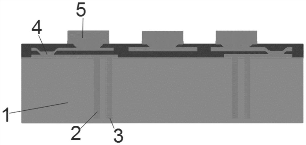
[0040] In this embodiment, the used wafer is a 4M asynchronous SRAM (static memory) wafer, which is finally a 3-layer SRAM wafer bonding product, such as Figure 5 shown. The 3-layer SRAM wafer bonding method includes the following steps: the process is as follows Figure 7 as shown,
[0041] Step 1. The first layer of wafer is only re-wiring and bump preparation on the front side, lead out the pad, and the front side is re-wiring to 3 layers, and the bump is electroplated SnAg, with a height of 3 μm;
[0042] The second layer wafer and the third layer wafer first complete the front rewiring and bump preparation, the number of rewiring layers is 3 layers, the front bump is electroplated Cu, and the height is 5 μm;
[0043] Step 2. The SnAg bumps on the front of the first layer of wafer are metal-bonded with the Cu bumps on the front of the second layer of wafer. The bonding temperature is 260°C, the time is 30 minutes, the bump opening ratio is 1.5%, and the bonding pressure...
Embodiment 2
[0052] Except the following content, all the other content are the same as embodiment 1.
[0053] The TSV diameter is 5 μm and the depth is 50 μm;
[0054] The bonding temperature is 240°C, the bonding time is 60min, the bump opening ratio is 3.5%, and the bonding pressure is 6000N;
[0055] The front rewiring layer is 2 layers, and the rear rewiring layer is 4 layers.
[0056] In step 5, in the metallization layer on the back of the second wafer, the adhesion layer is 0.5 μm Ti, the barrier layer is 1 μm Cu, and the wetting layer is 2 μm Ni;
[0057] In step 8, in the metallization layer on the back of the third wafer, the adhesion layer is 0.1 μm Ti, the barrier layer is 2 μm Cu, and the wetting layer is 5 μm Cu;
Embodiment 3
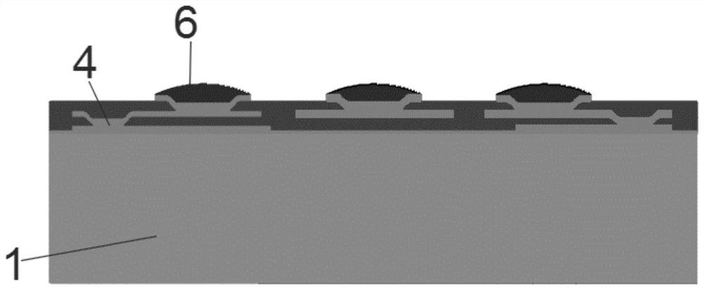
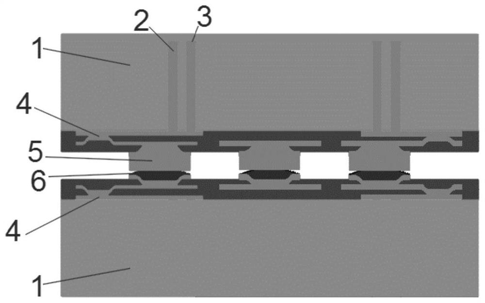
[0059] In this embodiment, the used wafer is a 4M asynchronous SRAM (static memory) wafer, and finally is a 5-layer SRAM wafer bonding product, such as Figure 6 As shown, the preparation process is as follows Figure 7 shown.
[0060] Step 1. The first layer of wafer is only re-wiring and bump preparation on the front side, lead out the pad, and the front side is re-wiring to 2 layers, and the bump is electroplated Cu, with a height of 3 μm;
[0061] The second layer wafer and the third layer wafer first complete the front rewiring and bump preparation, the number of rewiring layers is 3 layers, the front bump is electroplated Cu, and the height is 5 μm;
[0062] Step 2. The Cu bumps on the front side of the first layer wafer are metal-bonded with the Cu bumps on the front side of the second layer wafer. The bonding temperature is 400°C, the bonding time is 90 minutes, the bump opening ratio is 2%, and the bonding pressure is 20kN; through the Cu-Cu metal bonding process, t...
PUM
| Property | Measurement | Unit |
|---|---|---|
| Diameter | aaaaa | aaaaa |
| Depth | aaaaa | aaaaa |
| Thickness | aaaaa | aaaaa |
Abstract
Description
Claims
Application Information
 - R&D Engineer
- R&D Manager
- IP Professional
- Industry Leading Data Capabilities
- Powerful AI technology
- Patent DNA Extraction
Browse by: Latest US Patents, China's latest patents, Technical Efficacy Thesaurus, Application Domain, Technology Topic, Popular Technical Reports.
© 2024 PatSnap. All rights reserved.Legal|Privacy policy|Modern Slavery Act Transparency Statement|Sitemap|About US| Contact US: help@patsnap.com