Moving and transporting protection device for semiconductor device

A protection device, semiconductor technology, applied in the directions of transportation and packaging, containers, packaging, etc., can solve the problems of inconvenient placement and taking, falling off, pin bending, etc., to ensure the ventilation and filtration effect, easy to replace, easy to use The effect of device preservation

Active Publication Date: 2022-02-15
SHANGLUO UNIV
View PDF7 Cites 2 Cited by
  • Summary
  • Abstract
  • Description
  • Claims
  • Application Information

AI Technical Summary

Problems solved by technology

However, due to the structure of power semiconductor devices, vibrations will inevitably be caused when power semiconductor devices or chips are transported. If protection and shock absorption are not performed, the pins will be bent or virtual soldering will be caused, which will affect the performance of power semiconductors. The product quality of the device
[0004] The existing semiconductor device mobile transportation protection device clamps the semiconductor in the box through the clamping device, and is equipped with a spring shock absorbing component to achieve shock absorption, but it is not convenient to place and take. In the process, it is easy to cause bending or falling off of the pins of the semiconductor. For this reason, we propose a mobile transportation protection device for semiconductor devices

Method used


Image

  • Moving and transporting protection device for semiconductor device
  • Moving and transporting protection device for semiconductor device
  • Moving and transporting protection device for semiconductor device

Examples


Embodiment 1

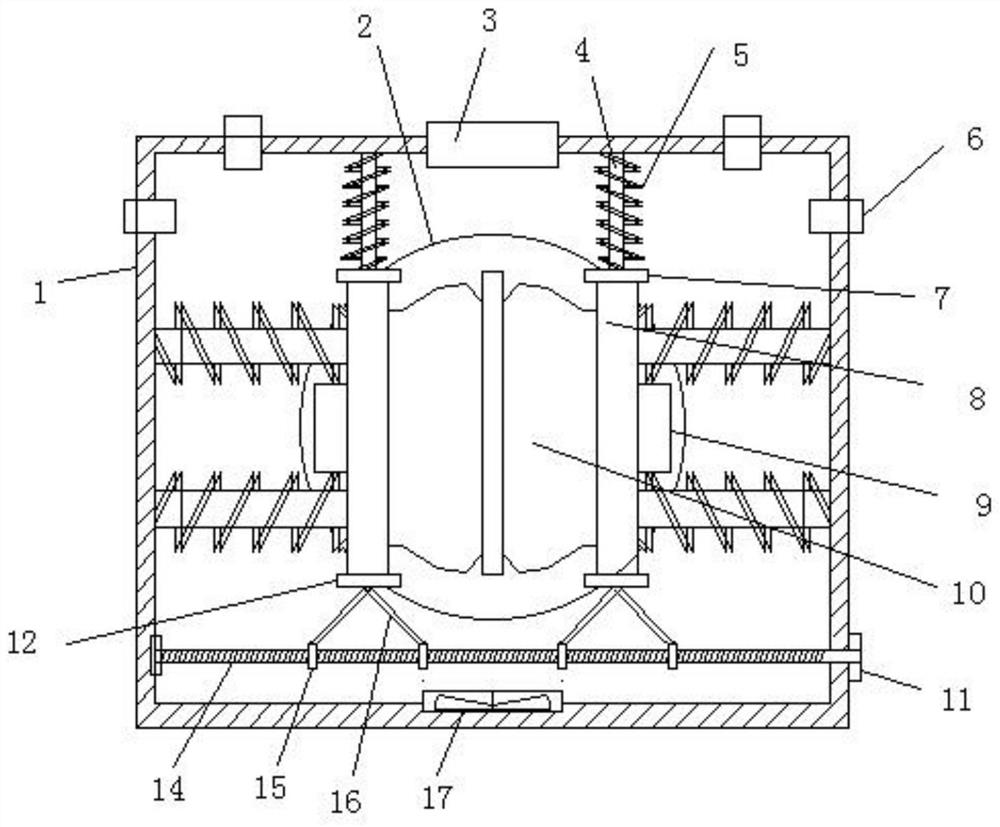
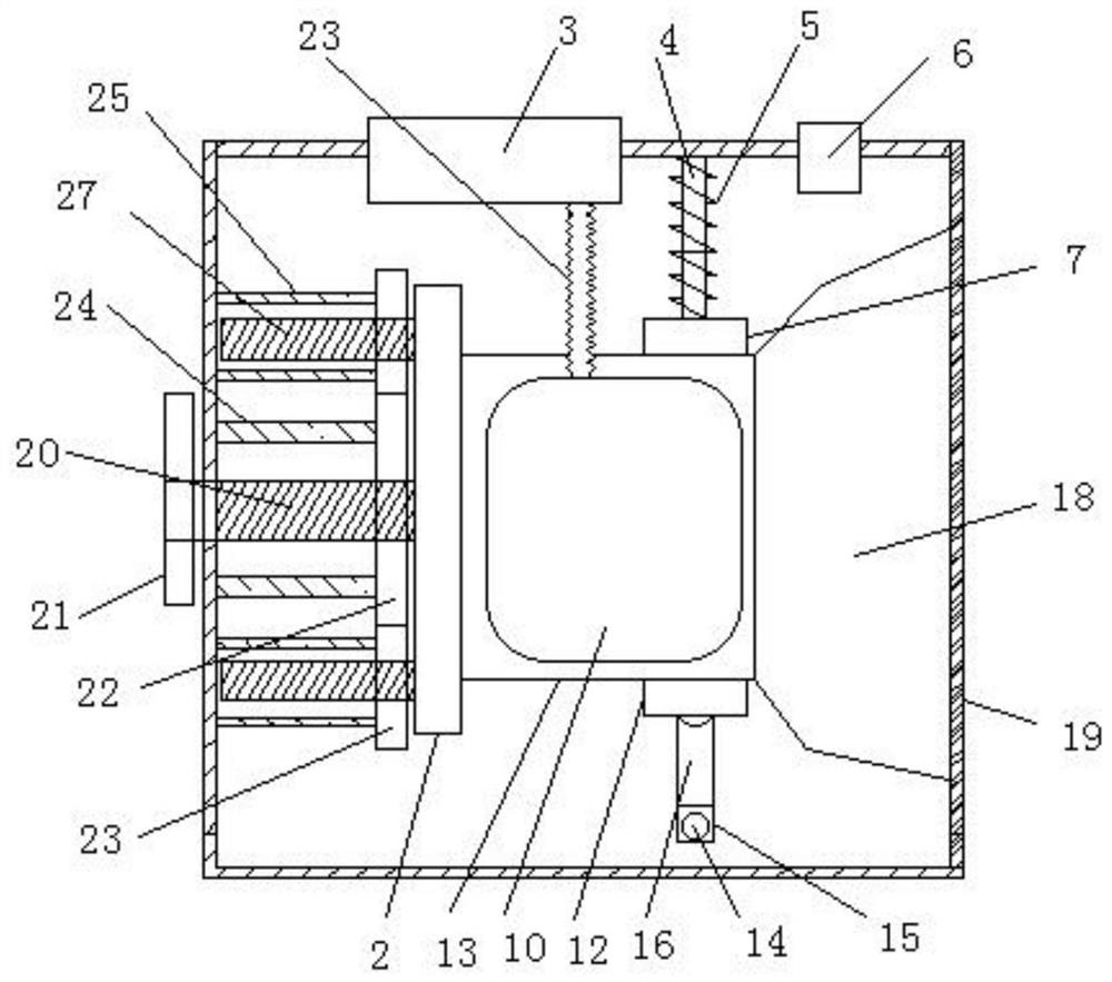
[0043] see figure 1 and figure 2 , a mobile transport protection device for semiconductor devices, including a protection box 1, the protection box 1 is movably connected to a dodge door 19, including;

[0044] The turntable 2 is arranged in the protection box 1, and the back of the turntable 2 is connected to the side wall of the protection box 1 through a push mechanism;

[0045] A set of clamping plates 8, a set of clamping plates 8 are symmetrically arranged on the turntable 2, a set of clamping plates 8 are respectively slidably connected with the turntable 2, and the clamping plates 8 are opposite to each other. The sides are respectively equipped with clamping protection components;

[0046] When specifically using the mobile transport protection device, open the dodge door 19 that is movably connected to the protection box 1, and then push the turntable 2 provided with the clamping plate 8 from the inside of the protection box 1 to the outside of the protection box ...

Embodiment 2

[0055] Further, in this embodiment, the clamping protection assembly includes two compressed airbags 10, which are respectively arranged on opposite sides of the two clamping plates 8, and the two compressed airbags 10 are respectively arranged on the protective box 1 The air suction pump 3 at the top communicates through the air supply pipe 13. When the semiconductor device needs to be clamped, the semiconductor device is placed between a set of clamping plates, then the air suction pump 3 is turned on, and the air is passed through the air supply pipe 13 Inflate the compressed airbags 10 until the compressed airbags 10 on both sides clamp the semiconductor device.

[0056] In order to facilitate the clamping of the semiconductor device by the compressed airbag, two interfering soft boards are included, which are respectively arranged on the opposite sides of the two compressed airbags 10, so as to prevent the contact surface of the compressed airbag 10 from being soft and aff...

Embodiment 3

[0067] Further, in order to ensure that the rotating disk 2 can be sent by the rotating push mechanism to open the dodge door 19 is pushed out of the protection box 1, so the dodge door 19 is opposite to the front of the turntable 2, and in order to ensure that the protection box 1 is in the closed state, the clamping plate 8 There is no gap between the dodge door 11, so the inside of the dodge door 11 is provided with a buffer air bag 18, and the buffer air bag 18 is in conflict with the end of the clamping plate 8 near the dodge door 19.

[0068] Further, in this embodiment, in order to ensure the ventilation of the wedding in the protective box 1, the protective box 1 also includes a fresh air system, because the semiconductor device storage environment requires certain requirements on temperature and humidity, so as to avoid damage to the semiconductor device, Therefore, a temperature and humidity sensor should be included for monitoring the temperature and humidity in the ...


PUM


Abstract

The invention relates to a semiconductor device moving and transporting protection device which comprises a protection box, a rotating disc is arranged in the protection box, two clamping plates are symmetrically arranged on the rotating disc and slidably connected with a disc, compressed air bags are arranged on the opposite sides of the two clamping plates respectively, and air supply boxes are arranged on the opposite sides of the two clamping plates. The air supply boxes are communicated with the compressed air bags, an air suction pump is arranged at the top of the protection box, and the air suction pump communicates with the air supply boxes through air supply pipes; spring compression parts are arranged on the side wall, close to the clamping plates, of the protection box, the clamping plates are connected with the side wall of the protection box through the spring compression parts, the back face of the rotating disc is connected with the side wall of the protection box through a rotating assembly, the side wall, opposite to the front face of the rotating disc, of the protection box is movably connected with a movable door, a fan is arranged at the bottom of the protection box, and a temperature and humidity sensor is arranged in the protection box.

Description

technical field [0001] The invention relates to the technical field of semiconductor device protection, in particular to a mobile transportation protection device for semiconductor devices. Background technique [0002] A semiconductor device is an electronic device whose conductivity is between a good conductor and an insulator. It uses the special electrical properties of semiconductor materials to complete specific functions. It can be used to generate, control, receive, transform, amplify signals and perform energy conversion. [0003] With the development of semiconductor-related technologies, the functions of chips are becoming more and more powerful, and the number of pins of semiconductor devices is increasing. In the production process of semiconductor devices, after the steps of mounting and fixing devices on the substrate and setting wires are completed, The device is often packaged, that is, the device is wrapped with a molding material such as epoxy resin moldin...

Claims


Application Information

Patent Timeline
Patent Type & Authority Applications(China)
IPC IPC(8): B65D25/10B65D81/05B65D81/07B65D81/26B65D85/86
CPCB65D25/101B65D81/052B65D81/07B65D81/263
Inventor 唐卫斌王博刘皎韩美林鱼轮
Owner SHANGLUO UNIV
Why Eureka
Try Eureka