
Light emitting device and method for modulating emission peak of light emitting device

A light-emitting device and emission peak technology, which is applied in semiconductor/solid-state device manufacturing, electric solid-state devices, semiconductor devices, etc., can solve the problems of poor repeatability and difficulty in adjusting the emission peak wavelength

Pending Publication Date: 2022-01-25
TCL CORPORATION
View PDF0 Cites 0 Cited by
  • Summary
  • Abstract
  • Description
  • Claims
  • Application Information

AI Technical Summary

Problems solved by technology

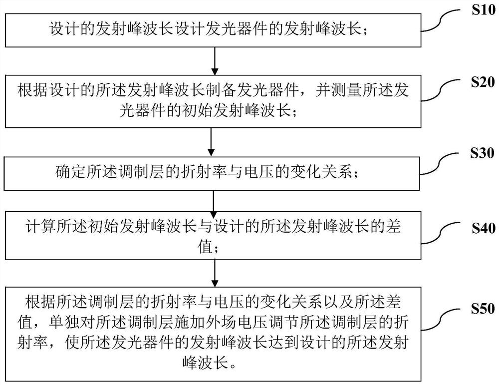
[0003] The purpose of the present invention is to provide a light-emitting device, which aims to solve the technical problems of high difficulty in adjusting the designed emission peak wavelength and poor repeatability of existing light-emitting devices to a certain extent.

Method used


Image

  • Light emitting device and method for modulating emission peak of light emitting device
  • Light emitting device and method for modulating emission peak of light emitting device
  • Light emitting device and method for modulating emission peak of light emitting device

Examples


Embodiment 1

[0069] A method for adjusting the emission peak of a light-emitting device, comprising the steps of:

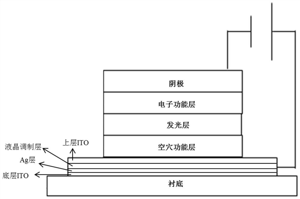
[0070] ①The emission peak wavelength of the light-emitting device is designed to be 624nm, according to the calculation formula of the theoretical emission peak wavelength of the light-emitting device: 1 / 2L λ =Σn i *d i , and the refractive index of ITO is 1.9, the refractive index of TFB is 1.8, the refractive index of QD is 1.9, and the refractive index of ZnO is 2.0. The thickness of each functional layer in the designed light-emitting device is: the thickness of ITO is 30nm; the thickness of TFB is 30nm; the thickness of QD The thickness of ZnO is 30nm; the thickness of ZnO is 30nm, and a modulation layer with a thickness of 80nm and a refractive index of 1.05 is introduced; at this time, 1 / 2L λ =1.05*80+1.9*30+1.8*30+1.9*30+2.0*30=312nm, then L λ =624nm, that is, the theoretical emission peak wavelength reaches the optimal emission wavelength of 624nm;

[0071] ② Pre...

Embodiment 2

[0077] A method for adjusting the emission peak of a light-emitting device as in embodiment 2, comprising the steps of:

[0078] ①The emission peak wavelength of the light-emitting device is designed to be 624nm, according to the calculation formula of the theoretical emission peak wavelength of the light-emitting device: 1 / 2L λ =Σn i *d i , and the refractive index of ITO is 1.9, the refractive index of TFB is 1.8, the refractive index of QD is 1.9, and the refractive index of ZnO is 2.0. The thickness of each functional layer in the designed light-emitting device is: the thickness of ITO is 30nm; the thickness of TFB is 30nm; the thickness of QD The thickness of ZnO is 30nm; the thickness of ZnO is 30nm, and a modulation layer with a thickness of 40nm and a refractive index of 2.2 is introduced; at this time, 1 / 2L λ =2.2*40+1.9*30+1.8*30+1.9*30+2.0*30=316nm, then L λ =632nm, that is, the theoretical emission peak wavelength reaches the optimal emission wavelength of 632nm...


PUM

PropertyMeasurementUnit
Thicknessaaaaaaaaaa
Thicknessaaaaaaaaaa
Thicknessaaaaaaaaaa

Abstract

The invention belongs to the technical field of display devices, and particularly relates to a light-emitting device which comprises a first electrode, a second electrode and a functional layer, the first electrode and the second electrode are oppositely arranged, and the functional layer is arranged between the first electrode and the second electrode and comprises a light-emitting layer. At least the first electrode comprises a metal layer and a first transparent conducting layer, the first transparent conducting layer is arranged on one side close to the functional layer, a modulation layer is further arranged between the metal layer and the first transparent conducting layer, and the refractive index of the modulation layer changes along with changes of external field voltage. According to the light-emitting device provided by the invention, the modulation layer is directly introduced into the electrode, so that the modulation layer participates in the microcavity effect of the device, the actual emission peak wavelength of the light-emitting device can approach and reach the preset emission peak wavelength, and the light-emitting efficiency of the device is improved.

Description

technical field [0001] The invention belongs to the technical field of display devices, in particular to a light emitting device and a method for modulating the emission peak of the light emitting device. Background technique [0002] As a new type of high-performance display device, quantum dot devices have the characteristics of high efficiency, narrow emission peak, and large Starks shift. But in common quantum dot devices, when the device is fabricated, the wavelength of the emission peak is fixed. In light-emitting devices, especially top-emitting quantum dot devices, due to the existence of F-P resonant microcavities, when the intrinsic wavelength of the material is close to the emission peak wavelength, the device performance is the best. Even for devices with the same material and structure, due to spin coating, evaporation and other processes and equipment capabilities, there will be some differences in each production, so that the emission peak wavelength of the m...

Claims


Application Information

Patent Timeline
IPC IPC(8): H01L51/52H01L51/50H01L51/56
CPCH10K50/115H10K50/81H10K50/852H10K50/858H10K71/00
Inventor 杨帆严怡然敖资通赖学森
Owner TCL CORPORATION
Learn More