Semiconductor structure and forming method of semiconductor structure

A semiconductor and nanostructure technology, which is applied in semiconductor devices, semiconductor/solid-state device manufacturing, transistors, etc., can solve the problems that the performance of fork-shaped nanosheets needs to be improved, and achieve the effect of simplifying the production process

Active Publication Date: 2022-01-25
SEMICON MFG INT (SHANGHAI) CORP +1
View PDF6 Cites 0 Cited by
  • Summary
  • Abstract
  • Description
  • Claims
  • Application Information

AI Technical Summary

Problems solved by technology

[0004] However, the performance of fork-shaped nanosheets needs to be improved

Method used


Image

  • Semiconductor structure and forming method of semiconductor structure
  • Semiconductor structure and forming method of semiconductor structure
  • Semiconductor structure and forming method of semiconductor structure

Examples


Embodiment Construction

[0031] As mentioned in the background art, the performance of the existing fork-shaped nanosheets still needs to be improved. Now analyze and illustrate in conjunction with specific embodiment.

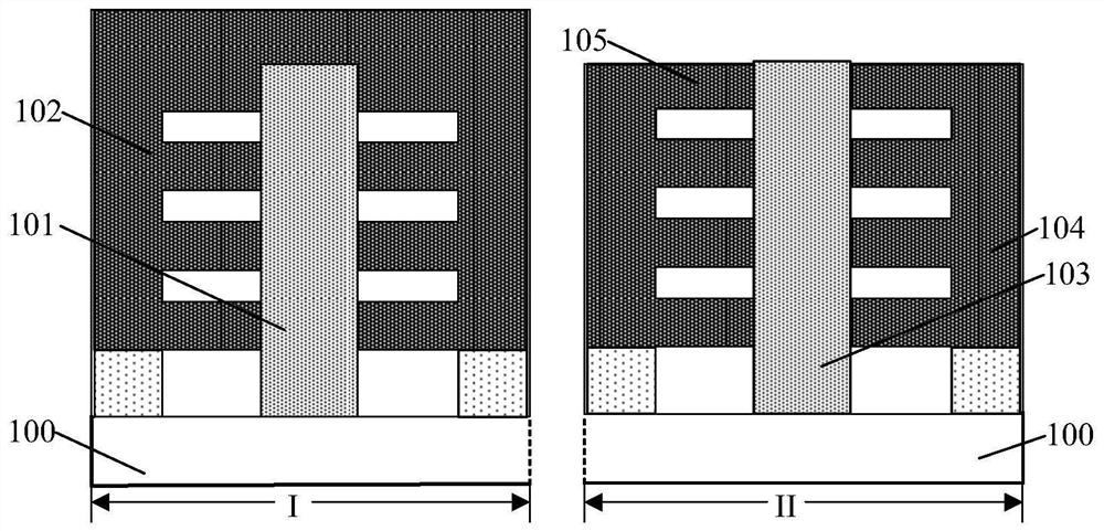
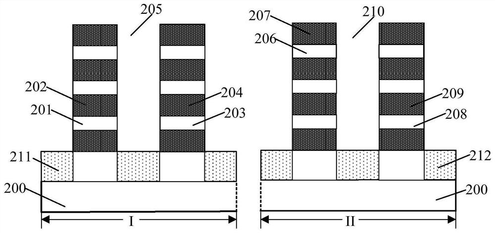
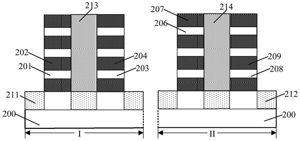
[0032] figure 1 It is a schematic cross-sectional structure diagram of a semiconductor structure in an embodiment.

[0033] Please refer to figure 1 , including: a substrate 100, the substrate 100 including a first region I and a second region II; a first isolation structure 101 located on the first region I, with first nanostructures on both sides of the first isolation structure 101 (not marked) and a second nanostructure (not marked); a second isolation structure 103 located on the second region II, the second isolation structure 103 has a third nanostructure (not marked) and a fourth nanostructure on both sides (not marked); the first gate structure 102 located on the first region 1, the first gate structure 102 straddles the first isolation structure 101, the first nanostructu...


PUM

PropertyMeasurementUnit
heightaaaaaaaaaa
widthaaaaaaaaaa
heightaaaaaaaaaa

Abstract

The invention discloses a semiconductor structure and a forming method of the semiconductor structure, and the structure comprises a substrate which comprises a first region and a second region; a first isolation structure which is located on the first region, and a first nanostructure and a second nanostructure which are located on the two sides of the first isolation structure respectively; a second isolation structure, wherein the top of the second isolation structure is lower than the top of the first isolation structure; a third nanostructure and a fourth nanostructure which are located on the two sides of the second isolation structure; a first gate structure and a second gate structure which are located on the first region, wherein the first gate structure and the second gate structure are exposed out of the top surface of the first isolation structure; and a third gate structure and a fourth gate structure on the second region, wherein the third gate structure and the fourth gate structure are in contact on the top surface of the second isolation structure. The formation of the semiconductor structure is improved.

Description

technical field [0001] The invention relates to the field of semiconductor manufacturing, in particular to a semiconductor structure and a method for forming the semiconductor structure. Background technique [0002] The Fin Field Effect Transistor (FinFET) architecture is the workhorse of today's semiconductor industry. However, as the device continues to shrink, when the channel length is small to a certain value, the FinFET structure cannot provide sufficient electrostatic control and sufficient driving current. Therefore, a nanosheet (Nanosheet) structure, that is, surround gate technology (Gate-All-Around, referred to as GAA, that is: ring gate), compared with FinFET, this ring-gate characteristic of nanosheets provides excellent channel control capabilities. At the same time, the excellent distribution of the channels in three dimensions enables the optimization of the effective driving current per unit area. [0003] With the demand for smaller track height (Track H...

Claims


Application Information

Patent Timeline
Patent Type & Authority Applications(China)
IPC IPC(8): H01L29/78H01L29/10H01L29/06H01L21/336
CPCH01L29/785H01L29/66795H01L29/0649H01L29/1033H01L21/823456H01L21/823481H01L27/088H01L27/092H01L21/823878H01L29/775H01L29/0673H01L29/66439B82Y10/00H01L27/124H01L27/1259
Inventor 陈建纪世良张海洋
Owner SEMICON MFG INT (SHANGHAI) CORP
Why Eureka
Try Eureka