
Piezoelectric substrate structure for filter and preparation method thereof

A substrate structure and filter technology, applied in the direction of electrical components, impedance networks, etc., can solve problems affecting the performance of piezoelectric substrate structures, and achieve the effects of avoiding bubble defects, improving acoustic resistance, and good adsorption

Active Publication Date: 2022-01-11
JINAN JINGZHENG ELECTRONICS
View PDF8 Cites 0 Cited by
  • Summary
  • Abstract
  • Description
  • Claims
  • Application Information

AI Technical Summary

Problems solved by technology

[0005] In order to solve the problem that in the prior art, when the piezoelectric substrate structure is prepared by bonding the piezoelectric film layer and the silicon oxide layer, a layer of water film is formed in the bonding surface, thereby affecting the performance of the piezoelectric substrate structure

Method used


Image

  • Piezoelectric substrate structure for filter and preparation method thereof
  • Piezoelectric substrate structure for filter and preparation method thereof
  • Piezoelectric substrate structure for filter and preparation method thereof

Examples


Embodiment Construction

[0041] In order to enable those skilled in the art to better understand the solutions of the present invention, the technical solutions in the embodiments of the present invention will be clearly and completely described below in conjunction with the drawings in the embodiments of the present invention.

[0042] The following will clearly and completely describe the technical solutions in the embodiments of the present invention with reference to the accompanying drawings in the embodiments of the present invention. Obviously, the described embodiments are only some, not all, embodiments of the present invention. Based on the embodiments of the present invention, all other embodiments obtained by those skilled in the art without creative efforts fall within the protection scope of the present invention.

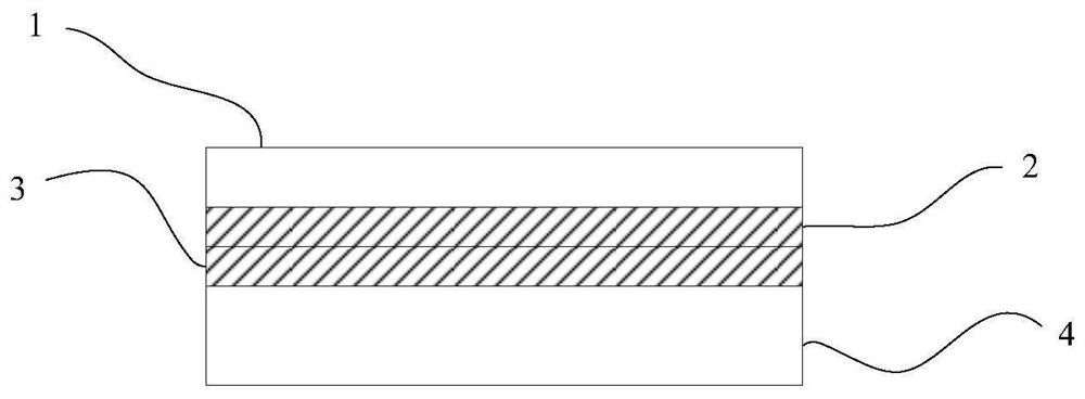
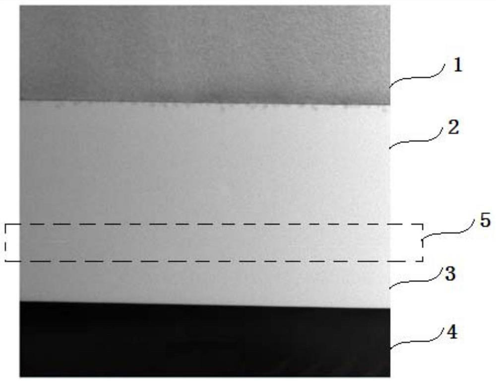
[0043] figure 1 A schematic structural diagram of a piezoelectric substrate structure for a filter provided by an embodiment of the present application is shown.

[0044] li...


PUM

PropertyMeasurementUnit
thicknessaaaaaaaaaa
thicknessaaaaaaaaaa
thicknessaaaaaaaaaa

Abstract

The embodiment of the invention discloses a piezoelectric substrate structure for a filter and a preparation method thereof, the piezoelectric substrate structure comprises a piezoelectric substrate, a first low acoustic resistance layer, a second low acoustic resistance layer and a support substrate which are stacked in sequence, and the surfaces of the first low acoustic resistance layer and the second low acoustic resistance layer are bonded after plasma activation. Water molecules between the first low-acoustic-resistance layer and the second low-acoustic-resistance layer can be diffused into the first low-acoustic-resistance layer and the second low-acoustic-resistance layer, so that the defect that the piezoelectric substrate generates bubbles due to the generation of water vapor is avoided; in addition, the existence of the first low-acoustic-resistance layer can effectively block proton exchange between H in water molecules between the first low-acoustic-resistance layer and the second low-acoustic-resistance layer and Li in the piezoelectric substrate, so that the original piezoelectric property of the piezoelectric substrate is ensured; moreover, since no water film exists between the piezoelectric substrate and the first low-acoustic-resistance layer, compared with the prior art, the acoustic resistance effect of the first low-acoustic-resistance layer and the second low-acoustic-resistance layer can be improved, and the radio-frequency signal loss of the surface acoustic wave filter can be reduced.

Description

technical field [0001] The present application relates to the field of semiconductor element preparation, in particular to a piezoelectric substrate structure for a filter and a preparation method thereof. Background technique [0002] The surface acoustic wave filter combines low insertion loss and good rejection performance. It can not only achieve wide bandwidth, but also has a much smaller volume than traditional filters, which can meet the needs of high integration. In the prior art, the piezoelectric substrate structure used in the surface acoustic wave filter includes, from top to bottom, a piezoelectric thin film layer, a low acoustic resistance layer (usually a silicon oxide layer), and a substrate layer. Among them, the role of low acoustic resistance is to block the signal in the piezoelectric film layer from leaking to the substrate layer, so as to reduce the loss of radio frequency signal of the surface acoustic wave filter. [0003] In the prior art, taking th...

Claims


Application Information

Patent Timeline
Patent Type & Authority Applications(China)
IPC IPC(8): H03H3/02H03H3/08H03H9/02H03H9/54H03H9/64
CPCH03H3/02H03H3/08H03H9/54H03H9/6489H03H9/02543H03H9/02818H03H2003/023
Inventor 李洋洋李真宇杨超张涛
Owner JINAN JINGZHENG ELECTRONICS
Learn More