
Fabrication method of gan-based micro-led structure and gan-based micro-led array

A manufacturing method and semiconductor technology, applied in semiconductor devices, electrical components, circuits, etc., can solve the problems of semiconductor layer and quantum well layer damage, affecting LED luminous efficiency, complex cutting process, etc., to overcome sidewall damage, cleavage The operation is easy to realize and overcome the effect of mass transfer

Active Publication Date: 2022-02-11
JIANGSU INST OF ADVANCED SEMICON CO LTD
View PDF3 Cites 0 Cited by
  • Summary
  • Abstract
  • Description
  • Claims
  • Application Information

AI Technical Summary

Problems solved by technology

However, on the one hand, such a solution may cause damage to the semiconductor layer and quantum well layer during the cutting process, especially the side wall damage directly affects the luminous efficiency of the LED; on the other hand, due to the small size of the micro LED, the cutting process is complicated and the cost higher
[0004] At the same time, when a sapphire substrate is used as the substrate of GaN micro-LEDs, there will be a certain stress between the substrate and the semiconductor layer due to lattice mismatch, and the crystal of the N-type semiconductor layer formed on the sapphire substrate The quality also needs to be improved, both stress and crystal quality have a great impact on LED luminous efficiency and service life

Method used


Image

  • Fabrication method of gan-based micro-led structure and gan-based micro-led array
  • Fabrication method of gan-based micro-led structure and gan-based micro-led array
  • Fabrication method of gan-based micro-led structure and gan-based micro-led array

Examples


Embodiment Construction

[0037] In view of the deficiencies in the prior art, the inventor of this case was able to propose the technical solution of the present invention after long-term research and extensive practice. The technical solution, its implementation process and principle will be further explained as follows.

[0038] A method for fabricating a GaN-based Micro-LED structure provided by one aspect of the present invention includes:

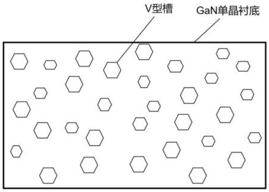
[0039] preparing a first semiconductor layer of the first conductivity type, wherein a plurality of depressions are formed on the surface of the first semiconductor layer, and the diameters and depths of the plurality of depressions are different;

[0040] A patterned mask is provided on the surface of the first semiconductor layer, and at least one first strip-shaped opening and at least one second strip-shaped opening are opened on the patterned mask, and the first strip-shaped opening and the second strip-shaped opening are The strip-shaped openings inters...


PUM

PropertyMeasurementUnit
thicknessaaaaaaaaaa

Abstract

The invention discloses a method for manufacturing a GaN-based Micro-LED structure and a GaN-based Micro-LED array. The manufacturing method includes: manufacturing an N-type GaN single crystal substrate with a plurality of V-shaped grooves formed on the surface; setting a patterned mask with a plurality of cross-shaped openings on the surface of the substrate, each cross-shaped opening formed by a first 1. The second strip-shaped openings are formed by intersecting each other, wherein the extending starting point of one of the first strip-shaped openings corresponds to the V-shaped groove with the largest diameter and depth at the edge of the substrate surface; the substrate is engraved using the mask etch to form a plurality of first and second line grooves intersecting each other on the surface of the substrate; remove the mask, and grow a quantum well layer and a p-type GaN layer on the surface of the substrate to form a stacked layer structure; use the first 1. The second slot is a cleavage line to cleavage the stacked layer structure. The invention can improve the light intensity of the Micro-LED and reduce the manufacturing difficulty thereof.

Description

technical field [0001] The invention relates to a method for manufacturing a Micro-LED, in particular to a method for manufacturing a GaN-based Micro-LED structure and a GaN-based Micro-LED array manufactured therefrom. Background technique [0002] With the increasing progress of LED epitaxial chip technology, Micro-LED (miniature light-emitting diode) as a pixel micro-LED display technology has become a popular development direction of the new generation of display technology. How to obtain better display effects on small-sized devices has become an urgent problem to be solved by many suppliers. With the reduction of the chip size and its unit spacing, the unit size of the chip is reduced to hundreds of microns to tens of microns, and the unit spacing is reduced to the level of ten microns, so that micro light-emitting diodes are facing challenges in terms of yield control and mass transfer technology. The challenge of design and equipment limit capability, these problems...

Claims


Application Information

Patent Timeline
Patent Type & Authority Patents(China)
IPC IPC(8): H01L33/00H01L33/12H01L27/15
CPCH01L33/0093H01L33/007H01L33/12H01L27/156
Inventor 王国斌刘宗亮
Owner JIANGSU INST OF ADVANCED SEMICON CO LTD
Learn More