Bias circuit, bias voltage regulation circuit, bias voltage regulation method and bias voltage regulation device

A technology of bias voltage adjustment and bias circuit, which is applied in the direction of adjusting electrical variables, control/regulation systems, instruments, etc., can solve the problems of large circuit volume, high additional cost, high complexity of bias circuit, etc., to reduce circuit complexity The effect of reducing extra cost and reducing circuit size

Pending Publication Date: 2021-11-30
SHENYANG NEUSOFT MEDICAL SYST CO LTD
View PDF7 Cites 1 Cited by
  • Summary
  • Abstract
  • Description
  • Claims
  • Application Information

AI Technical Summary

Problems solved by technology

[0005] In view of this, the present application provides a bias voltage circuit, a bias voltage adjustment circuit, a bias voltage adjustment method, a device, a storage medium, and a computer device, the main purpose of which is to solve the problem that the bias voltage of a semiconductor optoelectronic device cannot be independently set, and The technical problems of high complexity of bias circuit, bulky circuit and high additional cost

Method used


Image

  • Bias circuit, bias voltage regulation circuit, bias voltage regulation method and bias voltage regulation device
  • Bias circuit, bias voltage regulation circuit, bias voltage regulation method and bias voltage regulation device
  • Bias circuit, bias voltage regulation circuit, bias voltage regulation method and bias voltage regulation device

Examples


Embodiment Construction

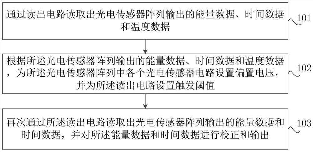
[0038] Hereinafter, the present invention will be described in detail with reference to the drawings and examples. It should be noted that, in the case of no conflict, the embodiments in the present application and the features in the embodiments can be combined with each other.

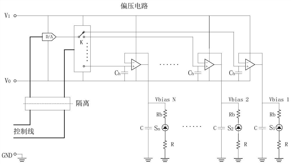
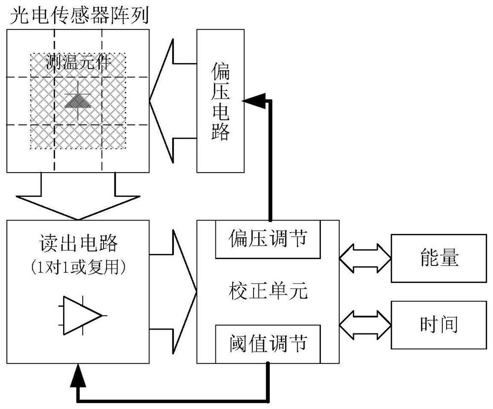
[0039] In the product design process of semiconductor optoelectronic devices, due to the discrete nature of the semiconductor process, even under the same bias voltage, the signal gain of each semiconductor optoelectronic device will have a large difference. In the prior art, in order to offset the discretization difference of semiconductor optoelectronic devices, the following two methods are mainly adopted.

[0040] The first method is to use a dedicated step-up DC-DC power module to adjust the bias voltage of the semiconductor optoelectronic device to make the gain consistent. The power module in this mode has only one output, which can uniformly adjust the bias voltage for multiple semiconductor...


PUM


Abstract

The invention discloses a bias circuit, a bias voltage regulation circuit, a bias voltage regulation method and a bias voltage regulation device. The bias circuit comprises a first constant voltage, a second constant voltage, a digital-to-analog converter, a multi-way switch and a plurality of holding circuits, wherein the digital-to-analog converter, the multi-way switch and the plurality of holding circuits are bridged between the first constant voltage and the second constant voltage, the input end of the digital-to-analog converter and the control end of the multi-way switch are respectively connected with a control bus, the output end of the digital-to-analog converter is connected with the input end of the multi-way switch, a plurality of output ends of the multi-way switch are respectively connected with the plurality of holding circuits, and the input end and the output end of each holding circuit respectively take thea first constant voltage and a grounding end as reference voltages; and the holding circuit can output corresponding bias voltage according to a voltage value input into the multi-way switch. According to the circuit, the output bias voltage can be independently adjusted for each holding circuit, a bias power supply module does not need to be independently provided, the circuit complexity is effectively reduced, the circuit size is reduced, and the extra cost is reduced.

Description

technical field [0001] The invention relates to the technical field of photoelectric sensors, in particular to a bias voltage circuit, a bias voltage adjustment circuit, a bias voltage adjustment method, a device, a storage medium and computer equipment. Background technique [0002] A semiconductor optoelectronic device refers to a semiconductor device that can convert light and electricity into each other. In the actual application process of semiconductor optoelectronic devices, their gain is easily affected by the bias voltage. At the same time, when using semiconductor optoelectronic devices to measure optical signals, the collected energy data and time data need to be highly accurate. Therefore, in product design, it is required that the signals of each semiconductor optoelectronic device in the photosensor array be consistent. However, due to the discrete nature of the semiconductor process, even under the same bias voltage, the signal gain of each semiconductor opto...

Claims


Application Information

Patent Timeline
IPC IPC(8): G05F1/567
CPCG05F1/567Y02P70/50
Inventor 张军杨龙梁国栋高鹏叶红杏
Owner SHENYANG NEUSOFT MEDICAL SYST CO LTD
Why Eureka
Try Eureka