


Quick Research
Generate reliable direction feasibility study reports for your R&D in just a few steps.

Technical Q&A
Discover and master advanced knowledge NOW. Basics, ideas, possibilities, all at once.

Find Solutions
As an expert in R&D theories, this can generate solutions to your technical problems instantly.

Evaluate Feasibility
Analyze your overall solution with one click, know your potential R&D risks in advance.

Monitor Landscape
Get weekly tech updates, stay abreast of the latest tech innovations and key insights.
Mixed light generation system for chip testing
A technology for generating systems and chip testing, applied in electronic circuit testing, single semiconductor device testing, optics, etc., can solve the problems of large light source size, inability to meet the requirements of chip testing speed, low testing efficiency, etc., to improve the testing efficiency. Effect
- Summary
- Abstract
- Description
- Claims
- Application Information
AI Technical Summary
Problems solved by technology
Method used
Image

Examples
no. 1 example
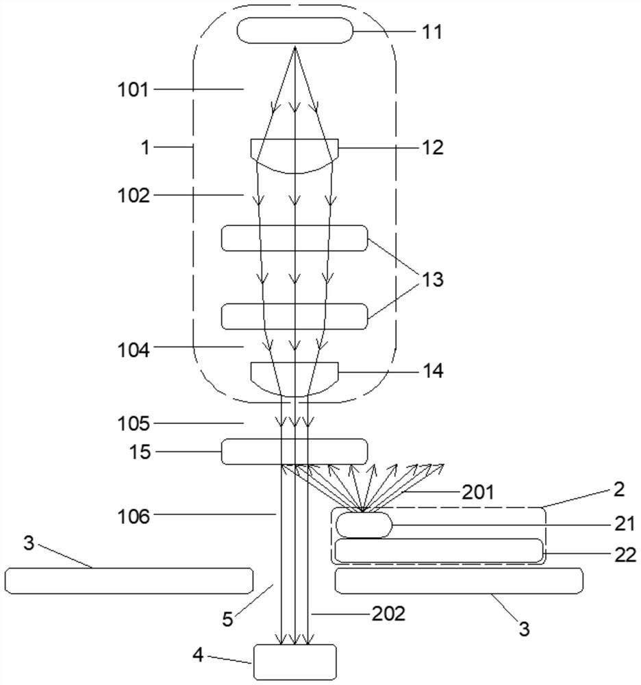
[0049] Such as figure 1 As shown, the DC optical module 1 includes a DC light source 11 and a DC optical drive control board. The DC optical drive control board has a DC drive circuit. The DC optical drive control board controls the power of the DC light emitted by the DC light source 11 by controlling the current. To realize the control of the output frequency of the DC light, the drive circuit of the DC light drive control board 11 in this embodiment is a light source control circuit commonly used in the field, as long as the control of the DC light can be realized, it will not be repeated here. The DC light source 11 generates a first DC optical path 101, and the first DC optical path 101 generates a second DC optical path 102 through the first collimating lens 12, and the second DC optical path 102 generates a fourth DC optical path 104 through the fly-eye lens assembly, and the fourth DC optical path The optical path 104 generates a fifth direct current optical path 105 t...
no. 2 example
[0053] Such as Figure 5 As shown, the overall hardware structure is the same as that of the first embodiment, except that the irradiation sequence of the optical path changes, that is, the direct current optical path is first irradiated on the grain photosensitive component 4, and the test probe card 3 collects the chip image under direct current light irradiation, Then the modulated light path is irradiated onto the photosensitive component 4 of the grain, and the test probe card 3 collects the chip image under the irradiated light by the modulated light.
no. 3 example
[0055] Such as Image 6 As shown, the overall hardware structure is the same as that of the first embodiment, except that the irradiation sequence of the optical path changes, that is, the modulated optical path is first irradiated onto the grain photosensitive component 4, and the test probe card 3 collects the chip image under the modulated light irradiation, Then the direct current light path is irradiated on the grain photosensitive part 4, and the test probe card 3 collects the chip image under the direct current light irradiation.
[0056] The above-mentioned first embodiment is to irradiate direct current light and modulated light at the same time, the second embodiment is to first direct current light, then modulate light, and the third embodiment is to first modulate light, and then direct current light, according to different embodiments, you can Get chip image information in different states.
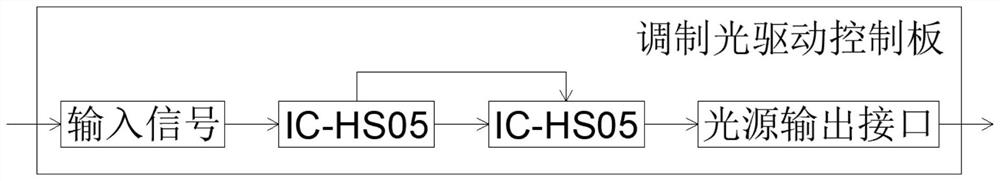
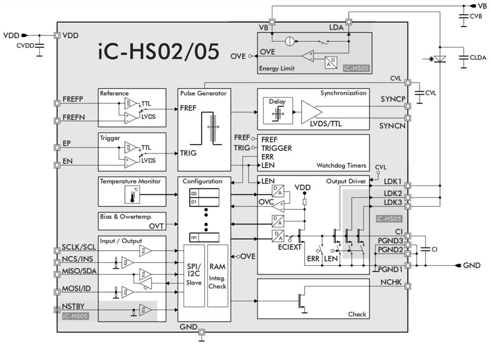
[0057] Such as figure 2 As shown, the modulation drive circuit is con...
PUM
| Property | Measurement | Unit |
|---|---|---|
| reflectance | aaaaa | aaaaa |
Abstract
Description
Claims
Application Information
 - R&D Engineer
- R&D Manager
- IP Professional
- Industry Leading Data Capabilities
- Powerful AI technology
- Patent DNA Extraction
Browse by: Latest US Patents, China's latest patents, Technical Efficacy Thesaurus, Application Domain, Technology Topic, Popular Technical Reports.
© 2024 PatSnap. All rights reserved.Legal|Privacy policy|Modern Slavery Act Transparency Statement|Sitemap|About US| Contact US: help@patsnap.com