Visible light communication cascade type array LED chip

An LED chip and visible light communication technology, applied in the field of visible light communication, can solve the problems of small light emitting area, limited light output power, low bandwidth, etc., and achieve the effects of improving stability, avoiding failure, and improving service life

Pending Publication Date: 2021-11-23
HEYUAN CHOICORE PHOTOELECTRIC TECH CO LTD
View PDF4 Cites 0 Cited by
  • Summary
  • Abstract
  • Description
  • Claims
  • Application Information

AI Technical Summary

Problems solved by technology

Large-sized LED chips often have low bandwidth due to high RC time constants, and small-sized LED chips limit their light output power because of their small light-emitting area.

Method used


Image

  • Visible light communication cascade type array LED chip
  • Visible light communication cascade type array LED chip
  • Visible light communication cascade type array LED chip

Examples


Embodiment 1

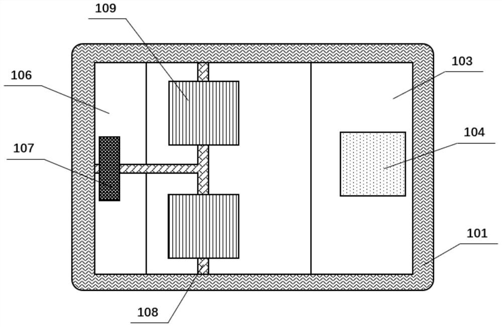
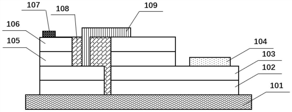
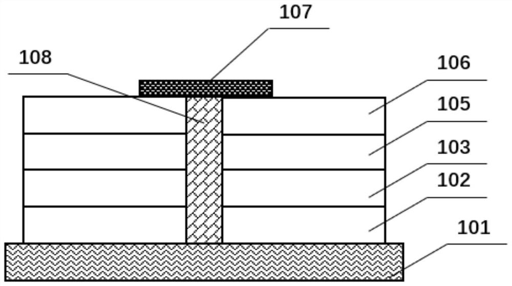
[0025] A visible light communication cascaded array LED chip, such as Figure 1 to Figure 3 As shown, it is composed of a large LED chip and an LED chip area connected in series. The LED chip area includes two small LED chips. An insulating layer 108 is provided between the large LED chip and the small LED chip and between adjacent small LED chips. , the large LED chip and each small LED chip include a functional layer, the functional layer is loaded on the surface of the substrate 101, and the functional layer includes a buffer layer 102 and an n-GaN layer 103 arranged in sequence from bottom to top , InGaN / GaN multi-quantum well layer 105 and p-GaN layer 106, the n-GaN layer 103 of the large LED chip is provided with an n-electrode 104, and the large LED chip and the small LED chip are connected by a metal bridge structure 109 One end of the metal bridge structure 109 is connected to the p-GaN layer 106 of the large LED chip, the other end of the metal bridge structure 109 i...

Embodiment 2

[0032] Provide a visible light communication cascaded array LED chip, such as Figure 4 As shown, it is composed of a large LED chip and an LED chip area connected in series. The LED chip area includes a plurality of small LED chips. An insulating layer 108 is provided between the large LED chip and the small LED chips and between adjacent small LED chips. , the large LED chip and each small LED chip include a functional layer, the functional layer is loaded on the surface of the substrate 101, and the functional layer includes a buffer layer 102 and an n-GaN layer 103 arranged in sequence from bottom to top , InGaN / GaN multi-quantum well layer 105 and p-GaN layer 106, the n-GaN layer 103 of the large LED chip is provided with an n-electrode 104, and the large LED chip and the small LED chip are connected by a metal bridge structure 109 One end of the metal bridge structure 109 is connected to the p-GaN layer 106 of the large LED chip, the other end of the metal bridge structu...


PUM

PropertyMeasurementUnit
heightaaaaaaaaaa
thicknessaaaaaaaaaa
thicknessaaaaaaaaaa

Abstract

The invention discloses a visible light communication cascade type array LED chip, and belongs to the technical field of visible light communication. The visible light communication cascade type array LED chip is formed by connecting an LED large chip and an LED chip area in series, the LED chip area comprises at least two LED small chips, insulating layers are arranged between the LED large chip and the LED small chips and between the adjacent LED small chips, the LED large chip and each LED small chip respectively comprise functional layers, the functional layers are loaded on the surface of a substrate, and the functional layer comprises a buffer layer, an n-GaN layer, a multi-quantum well layer and a p-GaN layer which are sequentially arranged from bottom to top. According to the invention, the plurality of small LED chips which are connected in parallel are connected in series with the large LED chip, and high current flowing through one large LED chip is uniformly distributed to the plurality of small LED chips which are connected in parallel at the next stage, so that the problem that the small LED chips fail due to overhigh current density is avoided, the overall stability of the chip structure is improved, and the service life of the LED is prolonged.

Description

technical field [0001] The invention belongs to the technical field of visible light communication, and in particular relates to a visible light communication cascaded array LED chip. Background technique [0002] In the past 30 years, the development of mobile communication has profoundly changed the way of life of human beings. Visible light communication (VLC) through the organic combination of lighting and communication technology, relying on its green environmental protection, harmless to the human body, no need for spectrum resources, and high confidentiality, can effectively solve the problem of traditional wireless network coverage, electromagnetic interference, information Safety and other issues are gradually becoming one of the candidate technologies for the next generation of mobile communications. [0003] In visible light communication, LED is an ideal light source due to its short response time and high-speed modulation. However, visible light communication ...

Claims


Application Information

Patent Timeline
Patent Type & Authority Applications(China)
IPC IPC(8): H01L27/15H01L33/62H01L33/06H01L33/12
CPCH01L27/15H01L33/62H01L33/06H01L33/12
Inventor 李国强
Owner HEYUAN CHOICORE PHOTOELECTRIC TECH CO LTD
Why Eureka
Try Eureka