
A kind of optoelectronic device and its preparation method

A photoelectric device and conductivity technology, applied in the field of photoelectric devices and their preparation, can solve problems hindering the development and application of quantum dot electroluminescent display technology, and achieve the effects of long service life, high luminous efficiency and high conductivity

Active Publication Date: 2022-05-20
ZHEJIANG UNIV +1
View PDF3 Cites 0 Cited by
  • Summary
  • Abstract
  • Description
  • Claims
  • Application Information

AI Technical Summary

Problems solved by technology

Although the performance of QLED devices in various aspects has been continuously improved in recent years, there is still a considerable gap between the basic device performance parameters such as device efficiency and device stability, and the requirements of industrial applications, which also greatly hinders the development of quantum LED technology. Development and Application of Dot Electroluminescence Display Technology

Method used


Image

  • A kind of optoelectronic device and its preparation method
  • A kind of optoelectronic device and its preparation method
  • A kind of optoelectronic device and its preparation method

Examples


preparation example Construction

[0049] The present invention also provides a method for preparing a photoelectric device, comprising the following steps: S1, providing a substrate, setting a first zinc oxide nanocrystal solution on the substrate, annealing to form a first electron transport layer; S2, forming a first electron transport layer on the first electron transport layer The second zinc oxide nanocrystal solution is placed on the substrate without annealing, and the second electron transport layer is formed after drying; or, S1, the substrate is provided, the second zinc oxide nanocrystal solution is placed on the substrate, and the second electron transport layer is formed by annealing treatment; S2, setting the first zinc oxide nanocrystal solution on the second electron transport layer, without annealing, forming the first electron transport layer after drying; wherein, the first zinc oxide nanocrystal has a first size, and the first zinc oxide nanocrystal The existence of the first defect state em...

Embodiment 1

[0059] (1) Synthesis of the first zinc oxide nanocrystals:

[0060] Synthesis of the third zinc oxide nanocrystal: Weigh 1mmol zinc acetate, dissolve it in 10mL dimethyl sulfoxide (DMSO), stir and dissolve at 50°C; continue to weigh 4mmol lithium hydroxide, and ultrasonically assist in dissolving it in 40mL ethanol solution; LiOH was completely dissolved, and it was directly injected into the DMSO solution containing zinc acetate, and reacted at 50°C for 1h.

[0061] The third surface treatment of zinc oxide nanocrystals: After the reaction is finished, add 2mmol acetic acid to neutralize the excess alkali in the reaction, and then add 0.5mmol Mg(Ac) to the system 2 DMSO (~5mL) solution, continue to react at 50°C for 30min.

[0062] Purification of the first zinc oxide nanocrystal: Take 5 mL of the above reaction stock solution, add 20 mL of ethyl acetate, centrifuge, pour off the supernatant; dissolve the precipitate with 1 mL of ethanol, add 3 mL of ethyl acetate, and centr...

Embodiment 2

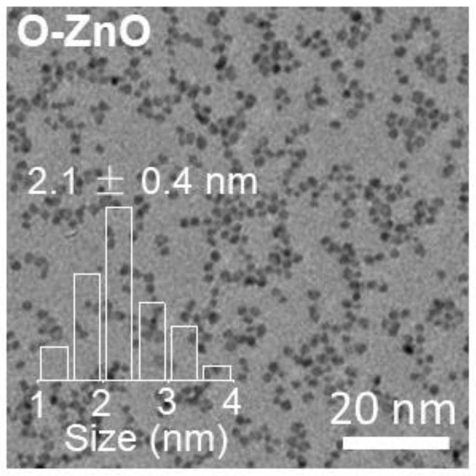
[0075] The difference between this embodiment and Example 1 is only: (1) the synthesis of the first zinc oxide nanocrystal: zinc acetate and Mg(Ac) 2 The ratio of the amount of substance is 5:1. The first zinc oxide nanocrystals with an average size of 2.2 nm were obtained.


PUM

PropertyMeasurementUnit
thicknessaaaaaaaaaa
current densityaaaaaaaaaa
sizeaaaaaaaaaa

Abstract

The invention provides a photoelectric device and a preparation method thereof. The photoelectric device comprises a substrate, a first electron transport layer and a second electron transport layer stacked in sequence, and the material of the first electron transport layer is the first zinc oxide nanocrystal, The material of the second electron transport layer is a second zinc oxide nanocrystal, the first zinc oxide nanocrystal has a first size, and the first zinc oxide nanocrystal has a first defect state light emission wavelength or does not exist a defect state light emission, which can suppress the substrate Exciton quenching at the interface with the first electron transport layer; the second zinc oxide nanocrystal has a second size, and the second zinc oxide nanocrystal has a second defect state light emission wavelength or does not exist defect state light emission, the first size and the second The two dimensions and the light emission wavelength of the first defect state and the second defect state light emission wavelength are all different, and the conductivity of the second zinc oxide nanocrystal is greater than that of the first zinc oxide nanocrystal. The photoelectric device of the present application has high luminous efficiency, long service life, stability in placement and operation.

Description

technical field [0001] The invention relates to the field of photoelectric technology, in particular to a photoelectric device and a preparation method thereof. Background technique [0002] Quantum dots are semiconductor nanocrystals with a size between 1-100nm and a "quantum confinement effect". Because quantum dots have a series of unique and excellent optical properties such as wide absorption spectrum, narrow emission fluorescence spectrum, and high luminescence quantum yield, they have broad application prospects in light-emitting diodes, solar cells, and bioluminescent labels. Especially in flat panel display applications, quantum dot electroluminescent diodes (Quantum dot light-emitting diodes, QLEDs) based on quantum dot materials have been used in display image quality, device performance, and manufacturing by virtue of the characteristics and optimization of quantum dot nanomaterials. Cost and other aspects have shown great potential. Although the performance of...

Claims


Application Information

Patent Timeline
Patent Type & Authority Patents(China)
IPC IPC(8): H01L51/50H01L51/54H01L51/56
CPCH10K71/40H10K50/115H10K50/166H10K2102/00H10K71/00Y02P70/50
Inventor 金一政陈德睢戴兴良陈栋
Owner ZHEJIANG UNIV
Learn More