Cold light luminous blister and hot pressing product and preparation method thereof
A hot-pressing and product technology, applied in the field of hot-pressing products and blistering, can solve the problems of low yield and high cost, and achieve the effects of high yield, changeable patterns and strong sense of technology.
- Summary
- Abstract
- Description
- Claims
- Application Information
AI Technical Summary
Problems solved by technology
Method used
Image
Examples
preparation example Construction
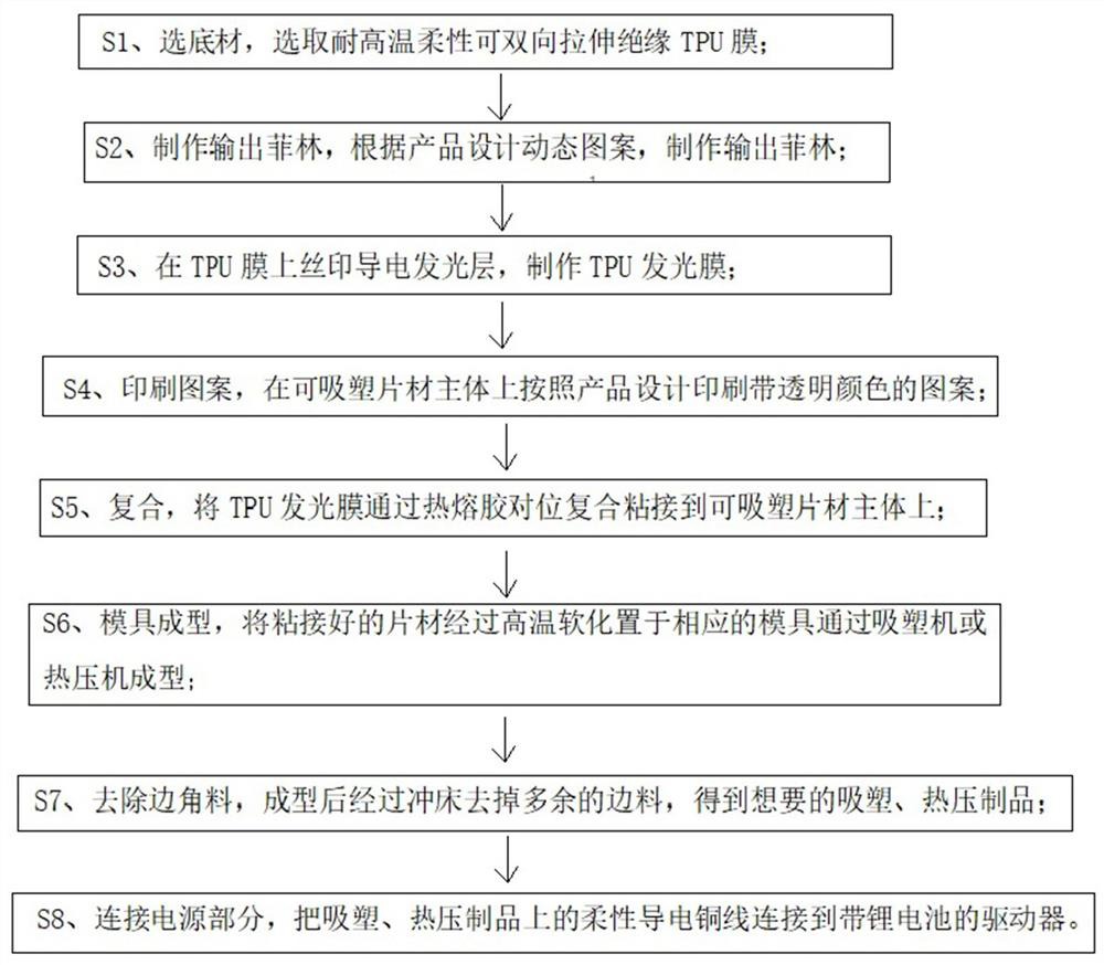
[0040] A method for preparing cold-light-emitting plastic-absorbing and hot-pressed products, comprising the following steps:
[0041] S1. Select the substrate, select high temperature resistant flexible biaxially stretchable insulating TPU film;
[0042] S2. Make the output film, design the dynamic pattern according to the product, and make the output film;
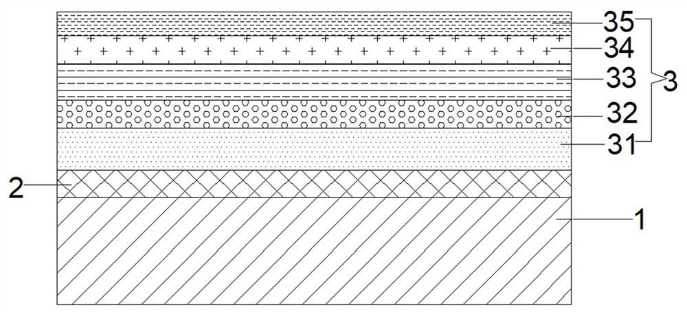
[0043] S3, screen-print the conductive luminescent layer 3 on the TPU film 2 to make a TPU luminescent film;
[0044] S4, printing patterns, printing patterns with transparent colors on the main body 1 of the blister sheet according to the product design;
[0045] S5, compounding, bonding the TPU light-emitting film to the main body 1 of the plastic-absorbing sheet through hot-melt adhesive compounding;
[0046] S6, mould-molding, the bonded sheet is softened at a high temperature and placed in a corresponding mold to form it through a blister machine or a hot press;
[0047] S7. Remove the leftover material, and remo...
Embodiment 1
[0057]Further, in step S301, the thickness of the positive electrode is 20 μm, and the screen printing method adopts 300 mesh screen printing.
[0058] Further, in step S302, the electroluminescent powder ZnS:Cu is mixed with dye, the ratio of ZnS:Cu to dye is 5:1, the thickness of the light-emitting layer is 40 μm, and the screen printing method adopts 150 mesh screen printing.
[0059] Further, in step S303, the thickness of the insulating layer is 30 μm, and the screen printing method adopts 150 mesh screen printing.
[0060] Further, in step S304, the thickness of the negative electrode is 20 μm, and the screen printing method adopts 200-mesh screen printing.
[0061] Further, in step S305, the thickness of the protective layer is 20 μm, and the screen printing method adopts 300-mesh screen printing.
Embodiment 2
[0063] Further, in step S301, the thickness of the positive electrode is 25 μm, and the screen printing method adopts 300 mesh screen printing.
[0064] Further, in step S302, the thickness of the light-emitting layer is 50 μm, and the screen printing method adopts 200 mesh screen printing.
[0065] Further, in step S303, the thickness of the insulating layer is 40 μm, and the screen printing method adopts 200-mesh screen printing.
[0066] Further, in step S304, the thickness of the negative electrode is 25 μm, and the screen printing method adopts 200-mesh screen printing.
[0067] Further, in step S305, the thickness of the protective layer is 25 μm, and the screen printing method adopts 300-mesh screen printing.
PUM
| Property | Measurement | Unit |
|---|---|---|
| thickness | aaaaa | aaaaa |
| thickness | aaaaa | aaaaa |
| thickness | aaaaa | aaaaa |
Abstract
Description
Claims
Application Information
 - R&D
- Intellectual Property
- Life Sciences
- Materials
- Tech Scout
- Unparalleled Data Quality
- Higher Quality Content
- 60% Fewer Hallucinations
Browse by: Latest US Patents, China's latest patents, Technical Efficacy Thesaurus, Application Domain, Technology Topic, Popular Technical Reports.
© 2025 PatSnap. All rights reserved.Legal|Privacy policy|Modern Slavery Act Transparency Statement|Sitemap|About US| Contact US: help@patsnap.com


