Microlens array
A micro-lens array and micro-lens technology, applied in the field of micro-optics, can solve problems such as the large influence of the micro-lens array, and achieve the effects of improving optical performance, expanding the adjustment range, and reducing the influence of optical performance.
- Summary
- Abstract
- Description
- Claims
- Application Information
AI Technical Summary
Problems solved by technology
Method used
Image

Examples
Embodiment 1
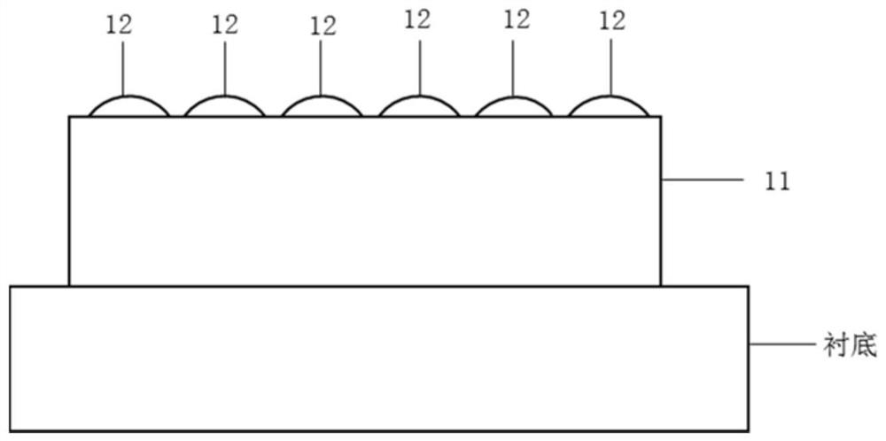
[0052] figure 1A schematic structural diagram of a microlens array provided by an embodiment of this specification.
[0053] Such as figure 1 As shown, the microlens array in this embodiment is located on the surface of the substrate, including: a platform structure 11 and a plurality of microlens structures 12 .
[0054] The platform structure 11 is located on the surface of the substrate.
[0055] A plurality of microlens structures 12 are arrayed above the platform structure 11 .
[0056] When the parallel incident light passes through the microlens array to cover the substrate surface, the height of the platform structure 11, the focal length of the microlens structure 12 and the area covered by the incident light on the substrate surface, the three satisfy the following relationship:
[0057] By separately setting the height of the platform structure 11 and the focal length of the microlens structure 12 , the parallel incident light passes through the microlens structu...
Embodiment 2
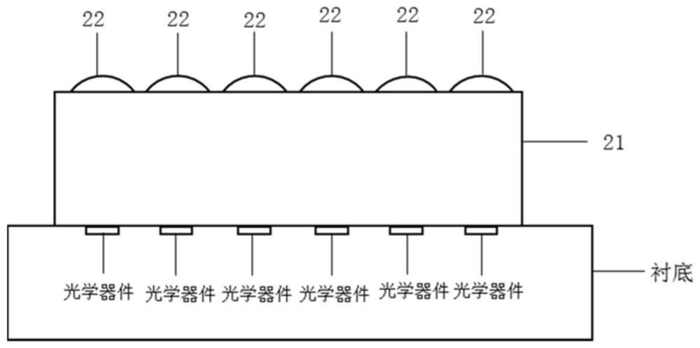
[0090] On the basis of Embodiment 1, Embodiment 2 of this specification provides a microlens array applied to the surface of a substrate on which an array of optical devices is formed.
[0091] In Embodiment 2, the same explanations are omitted for the same devices as in Embodiment 1. FIG.
[0092] figure 2 A schematic structural diagram of a microlens array provided by an embodiment of this specification.
[0093] Such as figure 2 As shown, the microlens array in this embodiment is located on the surface of the substrate, and includes a platform structure 21 and a plurality of microlens structures 22 .
[0094] An array of optical devices is formed on the surface of the substrate.
[0095] In the embodiment of this specification, the optical device includes at least one of a photosensitive device and a light source device.
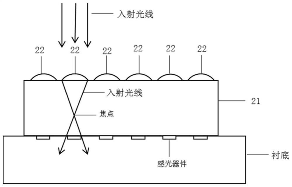
[0096]Wherein, the photosensitive device is used to receive incident light that passes through the microlens array and covers the surface of the su...
Embodiment 3
[0125] Vertical cavity surface emitting laser (VCSEL), as an important light source, can be used for low optical power data communication and parallel optical interconnection, as well as a series of high optical power applications, such as optical pumping, optical driving, 3D perception and LiDAR systems, etc. .
[0126] In practical applications, the large beam divergence angle of VCSEL arrays tends to reduce the far-field beam profile, which severely limits the working distance of VCSEL integrated systems. Therefore, VCSEL arrays usually need to be used in conjunction with external micro-optical components to improve their beam collimation or focus.
[0127] However, due to the size of the vertical cavity surface emitting laser and the thermal reflow process, the curvature diameter R and the crown height h of the microlens structure integrated on the substrate are determined to be small. L Higher, shorter focal length f, and larger intersection angle a lead to poor collimat...
PUM
 Abstract
Description
Claims
Application Information
 - R&D
- Intellectual Property
- Life Sciences
- Materials
- Tech Scout
- Unparalleled Data Quality
- Higher Quality Content
- 60% Fewer Hallucinations
Browse by: Latest US Patents, China's latest patents, Technical Efficacy Thesaurus, Application Domain, Technology Topic, Popular Technical Reports.
© 2025 PatSnap. All rights reserved.Legal|Privacy policy|Modern Slavery Act Transparency Statement|Sitemap|About US| Contact US: help@patsnap.com