Test key structure and wafer stacking structure

A stacking structure and test key technology, which is applied in semiconductor/solid-state device testing/measurement, electrical components, electric solid-state devices, etc., can solve the problems of inability to distinguish the order of test pads and ambiguity of related marks, so as to prevent human operation errors , reduced manpower, and the effect of saving test time

Pending Publication Date: 2021-08-17
WUHAN XINXIN SEMICON MFG CO LTD
View PDF0 Cites 0 Cited by
  • Summary
  • Abstract
  • Description
  • Claims
  • Application Information

AI Technical Summary

Problems solved by technology

Under the microscope, the relevant markings located on the front side are blurred, and the design of the evenly spaced test pads cannot distinguish the order of the test pads
And the order of the test pads of the upper and lower pieces is completely opposite. Without rewriting the test program, the test of the two pieces must be carried out separately.

Method used


Image

  • Test key structure and wafer stacking structure
  • Test key structure and wafer stacking structure
  • Test key structure and wafer stacking structure

Examples


Embodiment Construction

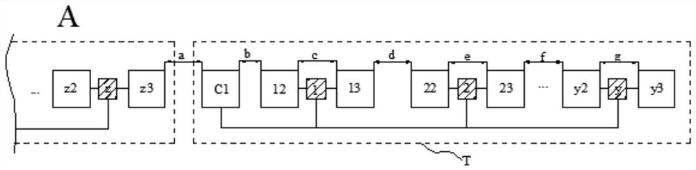
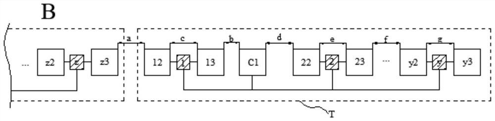
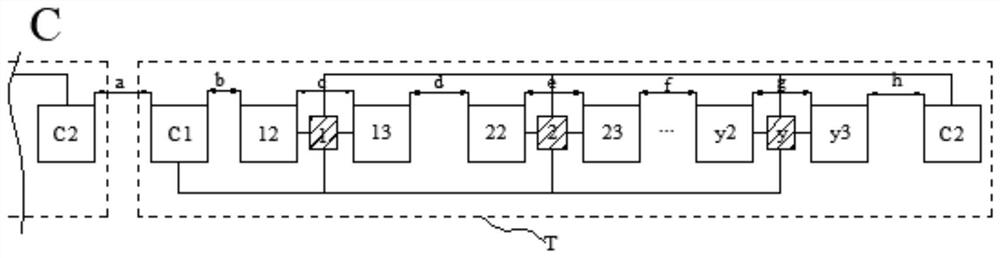
[0041] Based on the above research, an embodiment of the present invention provides a test key structure. The present invention will be described in further detail below in conjunction with the accompanying drawings and specific embodiments. The advantages and features of the present invention will become clearer from the following description. It should be noted that the drawings are all in a very simplified form and use imprecise scales, and are only used to facilitate and clearly assist the purpose of illustrating the embodiments of the present invention.

[0042] The embodiment of the present invention provides a test key structure, including:

[0043] At least one test key unit, the test key unit is distributed with several test elements to be tested and a plurality of test pads distributed at intervals, the distance between adjacent test pads is not completely the same, multiple test pads in the test key unit The test pad is asymmetric about the central axis of the tes...


PUM


Abstract

The invention provides a test key structure and a wafer stacking structure, and the structure comprises at least one test key unit, a plurality of to-be-tested elements and a plurality of test pads which are distributed at intervals are distributed on the test key unit, wherein the distances between the adjacent test pads are not completely the same, and the plurality of test pads in the test key unit are asymmetric with respect to the central axis of the test key unit. The distances between the adjacent test pads on the test key units are not completely the same, that is, the design of the test pads with non-uniform distances and asymmetric structures is adopted, so the sequence of the test pads on the test key units is easy to distinguish. The test key structure can be used for judging the sequence of the test pads by naked eyes, reduces the risk of errors when a test program is established, and can obviously reduce the time for removing faults. And the risk of man-made misoperation when the needle feeding position is confirmed is completely eradicated. The test programs of the single wafers are combined in the wafer stacking structure, so that the test time is saved, and the manpower for rewriting the test programs and the risk of errors are reduced.

Description

technical field [0001] The invention belongs to the technical field of integrated circuit manufacturing, and in particular relates to a test key structure and a wafer stacking structure. Background technique [0002] In the semiconductor process, in order to maintain the stability of product quality, it is necessary to continuously test the semiconductor components produced. Generally speaking, various semiconductor processes can be used to manufacture components on the die, and at the same time, the same steps can be used to manufacture the DUT and test pads on the dicing line of the wafer to simulate the same process on the die. The test key structure includes a number of test pads distributed at intervals of the test key unit. Use test devices such as probes to touch the test pads and measure various parameters of the test components to check whether the process is normal and effectively control product quality. [0003] For WAT (Wafer Acceptance Test, Wafer Acceptance ...

Claims


Application Information

Patent Timeline
Patent Type & Authority Applications(China)
IPC IPC(8): H01L23/58H01L23/48H01L21/66
CPCH01L23/58H01L23/48H01L22/14
Inventor 瞿奇
Owner WUHAN XINXIN SEMICON MFG CO LTD
Why Eureka
Try Eureka