Tunable array integrated broadband terahertz wave-absorbing resonatorbased on vanadium dioxide
A vanadium dioxide and terahertz technology, applied in the direction of electrical components, magnetic/electric field shielding, antennas, etc., can solve the problems of difficult adjustment, single tuning method, complicated preparation process, etc., and achieve the effect of active tuning and absorption
- Summary
- Abstract
- Description
- Claims
- Application Information
AI Technical Summary
Problems solved by technology
Method used
Image
Examples
Embodiment 1
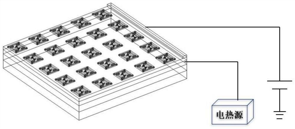
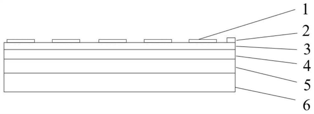
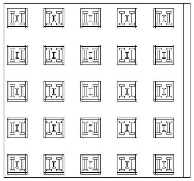
[0032] From bottom to top, the bottom metal layer Au (mainly for reflection) is a square structure with a side length of 50um and a thickness of 5um. The intermediate dielectric layer is made of Al 2 o 3 The layer is a square structure with a side length of 50um and a thickness of 1.9um. The upper layer is a vanadium dioxide phase change layer with a side length of 50um and a thickness of 2.5um. The upper layer is a graphene adjustable conductance layer. The rate layer is a square structure with a side length of 50um and a thickness of 1um. The top periodic array metasurface layer is an Al layer. Each unit structure is a square and the overall thickness is 1um. The outer length of the square is 6um, the wall thickness is 1.5um, and the inside is I-type resonant columns with the same shape but different sizes. The resonant columns are placed symmetrically along the center of the square. There are two types of I-type resonant columns, the larger The I-type resonant column is tw...
Embodiment 2
[0034] From bottom to top, the bottom metal layer Au (mainly for reflection) is a square structure with a side length of 60um and a thickness of 4um. The middle dielectric layer or lossy dielectric layer is made of SiO 2 The layer is a square structure with a side length of 60um and a thickness of 1.5um. The upper layer is a vanadium dioxide phase change layer with a side length of 60um and a thickness of 2.5um. The upper layer is a graphene adjustable conductance layer. The rate layer is a square structure with a side length of 60um and a thickness of 0.5um. The top periodic array metasurface layer is an Al layer. Each unit structure is square and the overall thickness is 1um. The outer length of the square is 7um, the wall thickness is 1um, and the interior is I-type resonant columns of different sizes with the same shape. The resonant columns are placed symmetrically along the center of the square. There are two types of I-type resonant columns. The type I resonance column ...
PUM
| Property | Measurement | Unit |
|---|---|---|
| electrical conductivity | aaaaa | aaaaa |
Abstract
Description
Claims
Application Information
 - R&D
- Intellectual Property
- Life Sciences
- Materials
- Tech Scout
- Unparalleled Data Quality
- Higher Quality Content
- 60% Fewer Hallucinations
Browse by: Latest US Patents, China's latest patents, Technical Efficacy Thesaurus, Application Domain, Technology Topic, Popular Technical Reports.
© 2025 PatSnap. All rights reserved.Legal|Privacy policy|Modern Slavery Act Transparency Statement|Sitemap|About US| Contact US: help@patsnap.com


