Wafer processing device, wafer conveying assembly and working method thereof

A technology for conveying components and processing devices, applied in the direction of conveyor objects, cleaning methods and tools, chemical instruments and methods, etc., which can solve problems such as wafer surface contamination, processing and processing process impact, wafer quality deterioration, etc.

Inactive Publication Date: 2021-08-03
CHANGXIN MEMORY TECH INC
View PDF8 Cites 1 Cited by
  • Summary
  • Abstract
  • Description
  • Claims
  • Application Information

AI Technical Summary

Problems solved by technology

[0003] However, the following cleanliness problems will exist in the process of transferring wafers by traditional robotic arms: for example, when the wafers are moved out of the process chamber, because some reactive gases (such as sulfur dioxide and fluorine gas) are still attached to the surface of the wafers, the The reaction gas will make the surface of the wafer easy to absorb the particles in the environment and cause the surface pollution of the wafer; in addition, the wafer will be affected by environmental factors, such as particles and metal ions in the environment will also adhere to the surface of the wafer, making the wafer surface The quality of the wafer deteriorates and affects the processing and handling process; in addition, when the wafer is directly exposed to the air during the transfer process, the surface of the wafer will be oxidized by oxygen in the air and a thin oxide film will be formed on the surface of the wafer, and The longer the transfer process takes, the longer the wafer is exposed to the air, and the more severely the surface of the wafer is oxidized

Method used


Image

  • Wafer processing device, wafer conveying assembly and working method thereof
  • Wafer processing device, wafer conveying assembly and working method thereof
  • Wafer processing device, wafer conveying assembly and working method thereof

Examples


Embodiment Construction

[0049] In order to make the above objects, features and advantages of the present invention more comprehensible, specific implementations of the present invention will be described in detail below in conjunction with the accompanying drawings. In the following description, numerous specific details are set forth in order to provide a thorough understanding of the present invention. However, the present invention can be implemented in many other ways different from those described here, and those skilled in the art can make similar improvements without departing from the connotation of the present invention, so the present invention is not limited by the specific embodiments disclosed below.

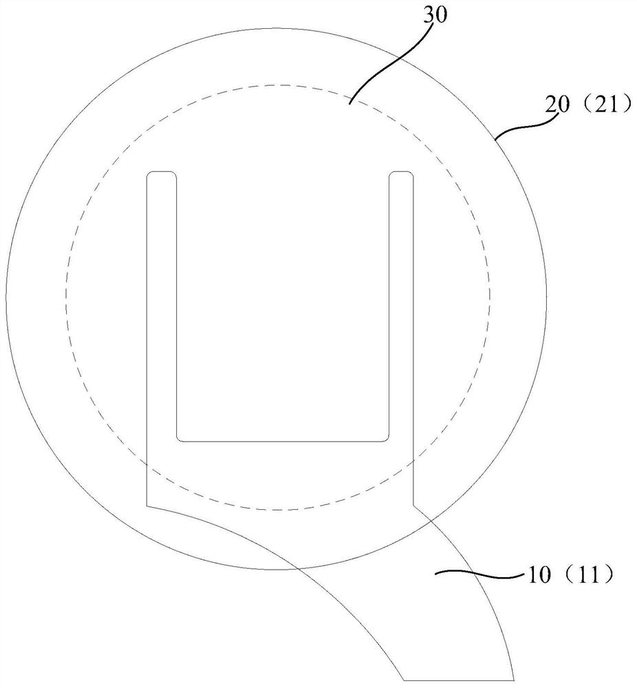
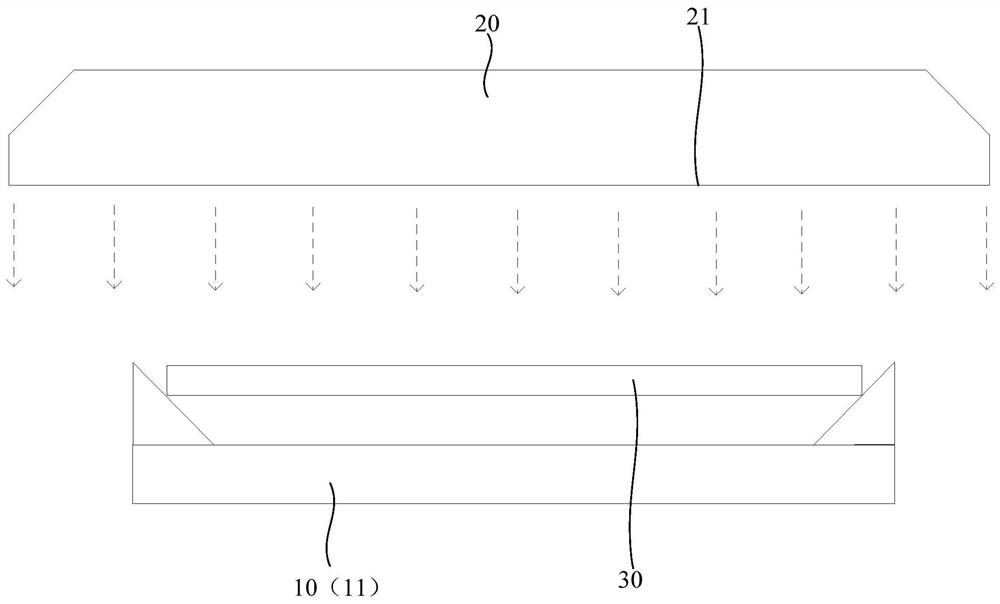
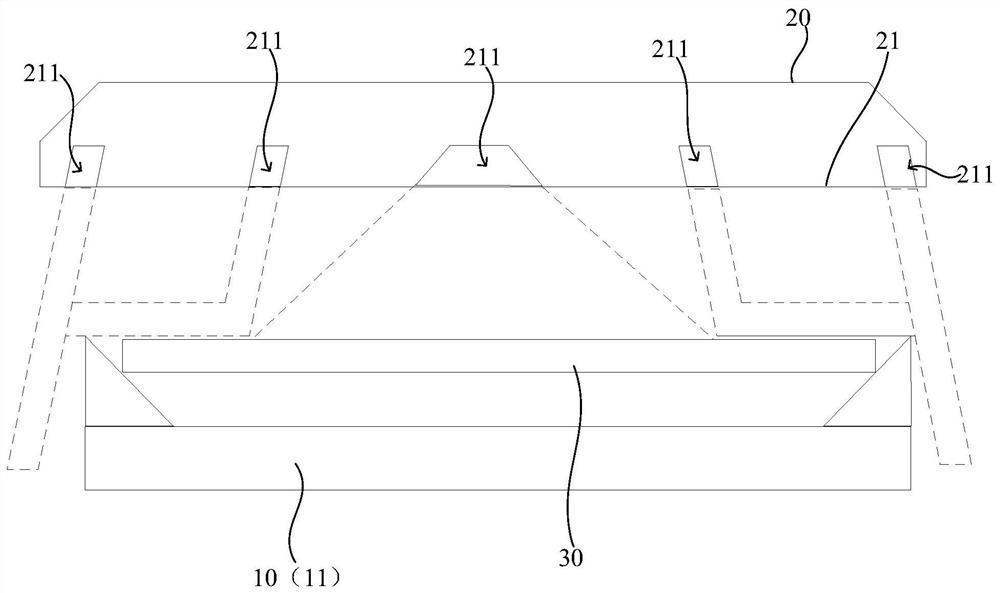
[0050] refer to figure 1 and figure 2 , figure 1 It shows a top structural schematic view of a wafer transfer assembly transferring a wafer 30 according to an embodiment of the present invention, figure 2 show figure 1 A schematic side view of an embodiment of the structure. An emb...


PUM


Abstract

The invention relates to a wafer processing device, a wafer conveying assembly and a working method thereof. The wafer conveying assembly comprises a moving mechanism and a purging structure. The moving mechanism comprises a tray. The tray can drive the wafer to move into the process chamber or move out of the process chamber. The purging mechanism is provided with a purging surface, and the purging area of the purging surface can completely cover the wafer placed on the tray. And when the tray of the moving mechanism drives the wafer to be positioned outside the process chamber, the purging mechanism is arranged right above the tray at an interval, so that the purging surface and the wafer on the tray are arranged in a face-to-face manner. In the process that the protective gas directly faces the wafer and purges the whole outer surface of the wafer, the pollution phenomenon that oxidation or particulate matter adheres to the surface of the wafer can be well avoided, it can be avoided that when the moving mechanism carries the wafer to move into the process cavity, water vapor is brought into the process cavity synchronously, and the surface cleanliness of the wafer can be guaranteed; and the surface of the wafer can be prevented from being oxidized, and the product quality is improved.

Description

technical field [0001] The invention relates to the technical field of semiconductor processing, in particular to a wafer processing device, a wafer transfer assembly and a working method thereof. Background technique [0002] In the wafer production process, a robot arm is usually used to move the wafer, so as to transfer the wafer from one position to another in space. For example, transferring wafers from a load chamber that stores wafers into a process chamber to process the wafers such as etching, or transferring wafers from one type of process chamber to another Types of process chambers to achieve different types of processing on wafers. [0003] However, the following cleanliness problems will exist in the process of transferring wafers by traditional robotic arms: for example, when the wafers are moved out of the process chamber, because some reactive gases (such as sulfur dioxide and fluorine gas) are still attached to the surface of the wafers, the The reaction ...

Claims


Application Information

Patent Timeline
Patent Type & Authority Applications(China)
IPC IPC(8): H01L21/677B08B5/02B08B13/00
CPCH01L21/67739B08B5/02B08B13/00
Inventor 金东镇
Owner CHANGXIN MEMORY TECH INC
Why Eureka
Try Eureka