Memory device and method of manufacturing same

A manufacturing method and technology for storage devices, which are applied in the fields of electric solid state devices, semiconductor devices, electrical components, etc., can solve the problems of compressing the process window, affecting the yield rate of semiconductor devices, and the inability of lithography machines to compensate.

Active Publication Date: 2021-07-30
YANGTZE MEMORY TECH CO LTD
View PDF7 Cites 0 Cited by
  • Summary
  • Abstract
  • Description
  • Claims
  • Application Information

AI Technical Summary

Problems solved by technology

For example, when etching silicon nitride-silicon oxide stacks (NO pairs) with a thickness of about 5 microns, the thickness of the mask needs to reach the order of microns. Alignment accuracy is compensated so that process results are only known after rework
At the same time, as the structure of 3D NAND devices becomes more complicated, the channel hole (Channel Hole) changes from single etching to secondary deposition and secondary etching. Increasing and becoming more serious problems such as hole tilting (tilting) are further compressing the process window and affecting the yield of semiconductor devices

Method used


Image

  • Memory device and method of manufacturing same
  • Memory device and method of manufacturing same
  • Memory device and method of manufacturing same

Examples


Embodiment Construction

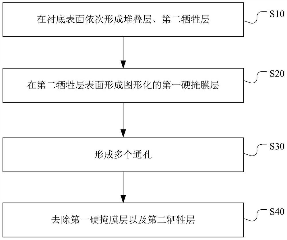
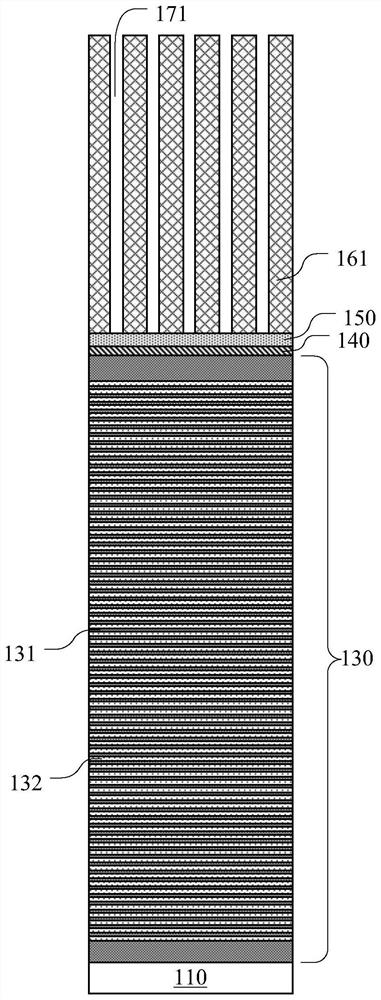
[0038] Hereinafter, the present invention will be described in more detail with reference to the accompanying drawings. In the various figures, identical elements are indicated with similar reference numerals. For the sake of clarity, various parts in the drawings have not been drawn to scale. Also, some well-known parts may not be shown in the drawings.

[0039] In the following, many specific details of the present invention, such as structures, materials, dimensions, processes and techniques of components, are described for a clearer understanding of the present invention. However, the invention may be practiced without these specific details, as will be understood by those skilled in the art.

[0040] It should be understood that when describing the structure of a component, when a layer or a region is referred to as being "on" or "over" another layer or another region, it may mean being directly on another layer or another region, or Other layers or regions are also in...


PUM

PropertyMeasurementUnit
thicknessaaaaaaaaaa
thicknessaaaaaaaaaa
thicknessaaaaaaaaaa

Abstract

The invention discloses a memory device and a manufacturing method thereof, and the manufacturing method comprises the steps: sequentially forming a stacking layer, a second sacrificial layer and a first hard mask layer on the surface of a substrate, the stacking layer comprising a plurality of first sacrificial layers and a plurality of interlayer insulating layers which are alternately stacked or comprising a plurality of grids and a plurality of interlayer insulating layers which are alternately stacked; forming a patterned first hard mask layer; forming a plurality of through holes penetrating through the stack layer and reaching the substrate; and removing the second sacrificial layer and the patterned first hard mask layer, wherein the first hard mask layer is a boron-doped amorphous carbon material layer. A boron-doped amorphous carbon material layer (Sophia) is adopted as the first hard mask layer, a pattern can be transferred to a stacking layer through the mask layer with a thinner thickness, and a photoetching machine can compensate overlay alignment precision at a current station in the photoetching process; therefore, photoetching can be completed with higher precision, and the problem of further compression of the photoetching window in the photoetching process is solved.

Description

technical field [0001] The present invention relates to the field of manufacturing storage devices, and more particularly, to a storage device and a manufacturing method thereof. Background technique [0002] As storage devices in semiconductor devices are widely used in daily life, people pay more and more attention to highly integrated electronic devices, and high-speed, low-power, high-density semiconductor storage devices are rapidly developed. 3D NAND device is an emerging flash memory developed by the industry. It solves the limitations brought by 2D NAND devices or planar NAND devices by vertically stacking multi-layer data storage units. It has higher precision and effectively reduces manufacturing costs. and energy consumption. Due to the increasing number of stacked layers of storage devices, the manufacture of important structural vias (Channel Holes) in the storage core area of ​​3D NAND devices requires higher process precision and greater aspect ratios. [00...

Claims


Application Information

Patent Timeline
Patent Type & Authority Applications(China)
IPC IPC(8): H01L27/11524H01L27/11551H01L27/1157H01L27/11578
CPCH10B41/20H10B41/35H10B43/20H10B43/35
Inventor 周毅张硕张伟
Owner YANGTZE MEMORY TECH CO LTD
Why Eureka
Try Eureka