Infrared light emitting diode epitaxial wafer and preparation method thereof

An infrared light-emitting and diode technology, which is applied in the direction of semiconductor devices, electrical components, circuits, etc., can solve problems such as the limited insulation capacity of gallium arsenide substrates, affecting the normal use of infrared light-emitting diode epitaxial wafers, and leakage, so as to reduce the leakage current Direct flow to the semi-insulating gallium arsenide substrate, ensuring stable use and avoiding the effect of conduction

Active Publication Date: 2021-07-23
HC SEMITEK SUZHOU
View PDF3 Cites 1 Cited by
  • Summary
  • Abstract
  • Description
  • Claims
  • Application Information

AI Technical Summary

Problems solved by technology

The semi-insulating gallium arsenide substrate has limited insulation capability, and it is prone to leakage to the semi-insulating gallium arsenide substrate, which affects the normal use of infrared light-emitting diode epitaxial wafers.

Method used


Image

  • Infrared light emitting diode epitaxial wafer and preparation method thereof
  • Infrared light emitting diode epitaxial wafer and preparation method thereof
  • Infrared light emitting diode epitaxial wafer and preparation method thereof

Examples


Embodiment Construction

[0024] In order to make the purpose, technical solution and advantages of the present disclosure clearer, the implementation manners of the present disclosure will be further described in detail below in conjunction with the accompanying drawings.

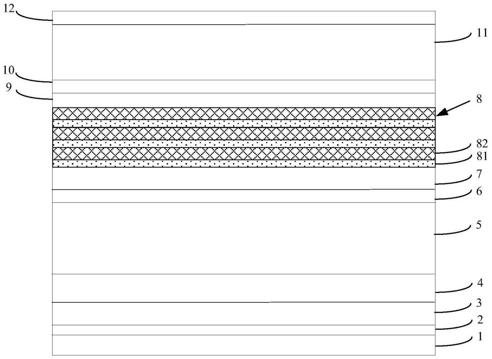
[0025] figure 1 It is a schematic structural diagram of a light-emitting diode chip provided by an embodiment of the present disclosure. Refer to figure 1 It can be seen that the embodiment of the present disclosure provides an infrared light-emitting diode epitaxial wafer, and the infrared light-emitting diode epitaxial wafer includes a semi-insulating gallium arsenide substrate 1 and a first intrinsic GaAs layer sequentially stacked on the semi-insulating gallium arsenide substrate 1 2. P-type GaAs layer 3, second intrinsic GaAs layer 4, n-type expansion layer 5, n-type confinement layer 6, n-plane waveguide layer 7, multiple quantum well layer 8, p-plane waveguide layer 9, p-type confinement layer 10. A p-type extension layer 1...


PUM

PropertyMeasurementUnit
temperatureaaaaaaaaaa
pressureaaaaaaaaaa
thicknessaaaaaaaaaa

Abstract

The invention provides an infrared light emitting diode epitaxial wafer and a preparation method thereof, which belong to the field of light emitting diode manufacturing. When the infrared light emitting diode epitaxial wafer is prepared, the substrate for growing the epitaxial layer is a semi-insulating gallium arsenide substrate, so that the substrate can be prevented from conducting electricity. The first intrinsic GaAs layer, the p-type GaAs layer and the second intrinsic GaAs layer are sequentially grown on the semi-insulating gallium arsenide substrate, and the overall conductivity is weak. And the p-type GaAs layer between the first intrinsic GaAs layer and the second intrinsic GaAs layer can play a role in consuming electrons and playing a role in blocking current, so that the situation that leakage current directly flows to the semi-insulating gallium arsenide substrate is reduced. What is ensured is that current stably flows in the epitaxial layer of the infrared light emitting diode epitaxial layer, and stable use of the finally obtained light emitting diode epitaxial wafer is ensured.

Description

technical field [0001] The disclosure relates to the field of light-emitting diode production, in particular to an infrared light-emitting diode epitaxial wafer and a preparation method thereof. Background technique [0002] A light-emitting diode chip is a semiconductor electronic component that emits light. As an efficient, environmentally friendly and green new solid-state lighting source, it is being rapidly and widely used, such as traffic lights, car interior and exterior lights, urban landscape lighting, mobile phone backlight, etc. Improving the luminous efficiency of light-emitting diode chips is the constant pursuit of light-emitting diodes. Target. [0003] Among various types of light-emitting diode chips, the epitaxial layer of the infrared light-emitting diode epitaxial wafer usually needs to be grown on the basis of a gallium arsenide substrate. The gallium arsenide substrate itself can be prepared from semi-insulating gallium arsenide, and the obtained epita...

Claims


Application Information

Patent Timeline
Patent Type & Authority Applications(China)
IPC IPC(8): H01L33/14H01L33/06H01L33/00
CPCH01L33/145H01L33/06H01L33/0062
Inventor 李彤王世俊邢振远
Owner HC SEMITEK SUZHOU
Why Eureka
Try Eureka