A fast response loop compensation circuit, loop compensation chip and switching power supply
A loop compensation, fast response technology, applied in electrical components, regulating electrical variables, output power conversion devices, etc., can solve the problems of high designer requirements, large debugging workload, output voltage overshoot, etc., to reduce stress, avoid output voltage overshoot, small area effect
- Summary
- Abstract
- Description
- Claims
- Application Information
AI Technical Summary
Problems solved by technology
Method used
Image


Examples
Embodiment 1
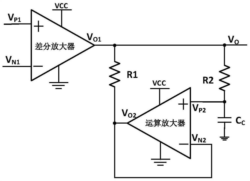
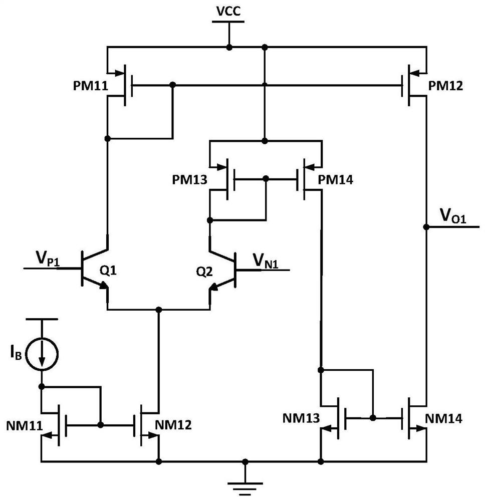
[0040] like Image 6 Shown is the principle block diagram of the first implementation of the fast-response loop compensation circuit of the present invention, including: a variable output slew rate differential amplifier, a dynamic current sensing operational amplifier, a zero-point resistor R1, a pole-point resistor R2, and a compensation capacitor C C. The signal input positive port 101 of the variable output slew rate differential amplifier is used as the signal input positive port of the fast response loop compensation circuit. The signal input negative port 102 of the variable output slew rate differential amplifier is used as the signal input negative port of the fast response loop compensation circuit, and the voltage difference between the ports 101 and 102 is the input voltage of the fast response loop compensation circuit. The voltage input positive port 103 of the variable output slew rate differential amplifier is connected to the positive VCC of the power supply,...
Embodiment 2
[0071] like Figure 7 shown is a schematic block diagram of the second implementation of the fast response loop compensation circuit of the present invention. On the basis of the first embodiment, a low transconductance differential amplifier is added, and the signal input positive port 201 of the low transconductance differential amplifier is connected to the The signal input positive port 101 of the variable output slew rate differential amplifier is connected to the signal input positive port of the fast response loop compensation circuit, and its signal input negative port 202 is in phase with the signal input negative port 102 of the variable output slew rate differential amplifier. connected, as the signal input negative port of the fast response loop compensation circuit, its output port 205 is connected with the output end 111 of the dynamic current sense operational amplifier, its voltage input positive port 203 is connected with the power supply positive VCC, its volt...
Embodiment 3
[0079] This embodiment provides a loop compensation chip, such as Figure 14 As shown, the fast response loop compensation circuit of the first embodiment or the second embodiment is included. The loop compensation chip includes at least a high voltage power input positive pin VDD (port 401), a low voltage power output pin VCC (port 402), a feedback voltage input pin FB (port 403), and a power input negative pin GND (port 404) , Soft-start time setting pin SS (port 405), optocoupler drive pin V Opt (port 406).
[0080] The loop compensation chip of the present invention also includes a reference voltage source generating circuit, an optocoupler driving tube PM0, and a soft-start resistor R SS , soft-start cut-off diode D SS . The input end of the reference voltage source generation circuit is connected to the high-voltage power input positive pin VDD, the first output end of the reference voltage source generation circuit is connected to the signal input positive port of t...
PUM
 Abstract
Description
Claims
Application Information
 - R&D
- Intellectual Property
- Life Sciences
- Materials
- Tech Scout
- Unparalleled Data Quality
- Higher Quality Content
- 60% Fewer Hallucinations
Browse by: Latest US Patents, China's latest patents, Technical Efficacy Thesaurus, Application Domain, Technology Topic, Popular Technical Reports.
© 2025 PatSnap. All rights reserved.Legal|Privacy policy|Modern Slavery Act Transparency Statement|Sitemap|About US| Contact US: help@patsnap.com