Optical element unit

A technology of optical components and optical systems, applied in the direction of optical components, optics, connecting components, etc., can solve problems such as a large amount of time and easy enlargement of laser processing equipment

Pending Publication Date: 2021-06-25
DISCO CORP
View PDF1 Cites 0 Cited by
  • Summary
  • Abstract
  • Description
  • Claims
  • Application Information

AI Technical Summary

Problems solved by technology

However, this method requires a lot of time in the measurement of deformation, and on the other hand, it cannot fundamentally suppress the occurrence of problems caused by deformation.
If a larger optical element is used, the influence of deformation can be relatively reduced, but in this case, the laser processing device is likely to be enlarged
Moreover, it is not easy to use larger optical elements when improving the optical system of the existing laser processing device

Method used


Image

  • Optical element unit
  • Optical element unit
  • Optical element unit

Examples


Embodiment Construction

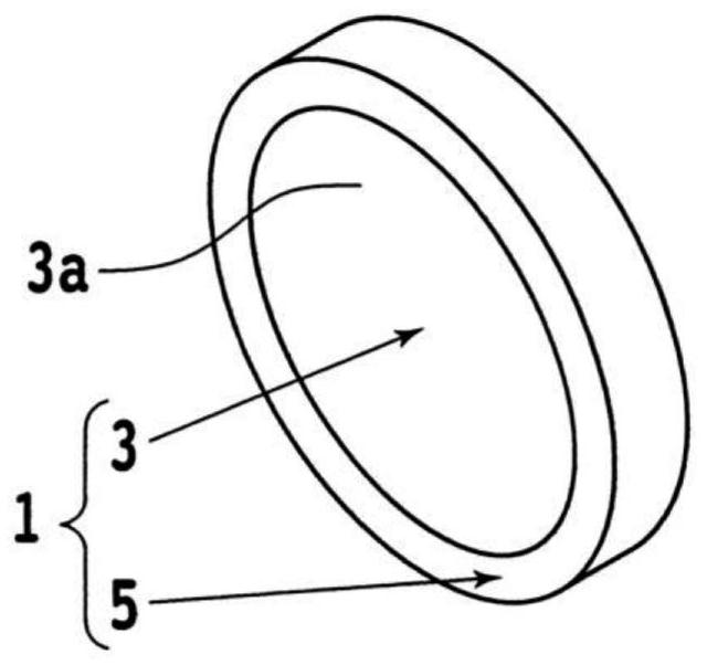
[0027] Embodiments of the present invention will be described with reference to the drawings. figure 1 It is a perspective view of the optical element unit 1 of this embodiment. Such as figure 1 As shown, the optical element unit 1 includes a disc-shaped reflective optical element 3 and a support body 5 that supports the outer peripheral portion of the optical element 3 . The optical element 3 is typically a mirror or the like, and has a front surface 3a on which light is incident. The optical element 3 is arranged, for example, at a predetermined position in an optical system constituting a laser processing apparatus (not shown) or the like.

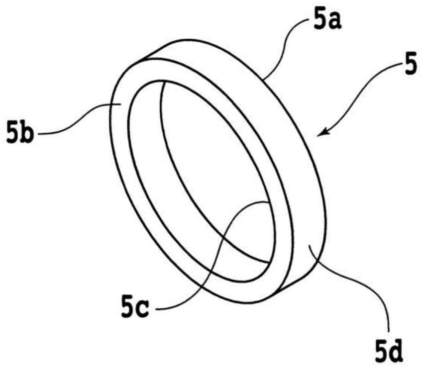
[0028] figure 2 is a perspective view of the support body 5 included in the optical element unit 1, image 3 is from with figure 2 The perspective view of the carrier 5 is viewed from the opposite direction. The support body 5 is formed into a cylindrical shape using, for example, aluminum, and has a first surface 5 a correspond...


PUM


Abstract

The invention provides an optical element unit, which can construct an optical system with high precision even when a conventional fixing tool is used. The optical element unit includes: a reflective optical element; and a support body for supporting the optical element, the support body being fixed by a fixing tool when the optical element is disposed at a predetermined position in the optical system. The support body is fixed by the fixing tool, so that the deformation of the optical element is alleviated compared with the situation that the optical element is directly fixed by the fixing tool.

Description

technical field [0001] The present invention relates to an optical element unit including a reflective optical element typified by a mirror. Background technique [0002] When dividing a plate-shaped workpiece represented by a semiconductor wafer into a plurality of chips, a laser processing apparatus including optical elements such as a laser oscillator, mirrors, and lenses is sometimes used (for example, refer to Patent Document 1). By irradiating a laser beam generated by a laser oscillator through various optical elements to the streets (segmentation planning lines) of the workpiece which are the boundaries of the chips, the workpiece can be divided into a plurality of chips by the streets. [0003] Patent Document 1: Japanese Patent Laid-Open No. 2007-275912 [0004] Moreover, when constructing the optical system of the said laser processing apparatus, for example, the optical element is arrange|positioned in the predetermined position of an optical system using the fi...

Claims


Application Information

Patent Timeline
Patent Type & Authority Applications(China)
IPC IPC(8): G02B7/00B23K26/70B23K26/06
CPCB23K26/0643B23K26/702G02B7/00G02B7/02G02B7/025G02B7/026G02B7/182F16B47/003
Inventor 大町修出岛健志九鬼润一
Owner DISCO CORP
Why Eureka
Try Eureka