
Half-hole plate one-time molding processing method and printed circuit board

A technology of molding processing and half-hole plate, which is applied to printed circuit parts and mechanically removes conductive materials, etc., can solve problems affecting production efficiency, damage to gongs and knives, increase processing flow and production costs, etc., and achieve improvement Accurate speed, improve molding accuracy, and save manpower

Active Publication Date: 2021-09-21
四川英创力电子科技股份有限公司
View PDF5 Cites 0 Cited by
  • Summary
  • Abstract
  • Description
  • Claims
  • Application Information

AI Technical Summary

Problems solved by technology

The main defect of this method is that half-holes are formed before solder masking, hollow areas appear on the board surface, and the structural strength of the board is reduced, which increases the difficulty of solder mask silk screen printing. cost, and also affects production efficiency
In addition, in the process of semi-orifice board processing, the circuit board is thin, and the timing of the lowering and lifting of the gong knife is difficult to be accurate, and it may cut to the platform below the circuit board, causing damage to the gong knife

Method used


Image

  • Half-hole plate one-time molding processing method and printed circuit board
  • Half-hole plate one-time molding processing method and printed circuit board
  • Half-hole plate one-time molding processing method and printed circuit board

Examples


Embodiment 1

[0067] As an aspect of the embodiment of the present application, there is provided a one-time molding processing method for a half-hole plate, including steps: pretreatment, drilling, copper sinking / plate electrical, outer layer circuit, graphic plating, etching, solder mask, text, surface Processing, forming.

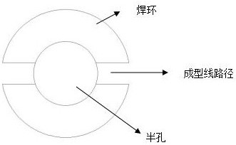
[0068] Wherein, in this example, the etching step uses etching solution to remove the copper on the molding line path in the half-hole solder ring, such as figure 1 shown.

[0069] Wherein, in this example, the molding step includes:

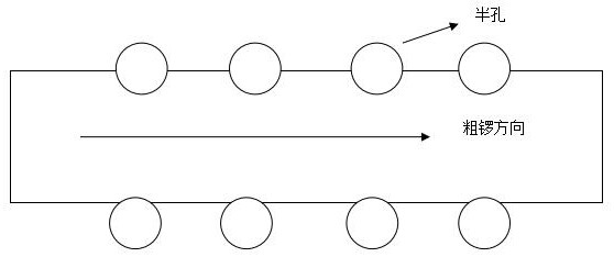
[0070] S100, thick gong: such as figure 2 As shown, the circuit board is slotted through thick holes, and the thick holes are drilled from between the half holes on both sides of the circuit board, and the grooves are not reached during the thick hole.

[0071] S200. Fix the circuit board on the cardboard, and the cardboard is used to support the circuit board.

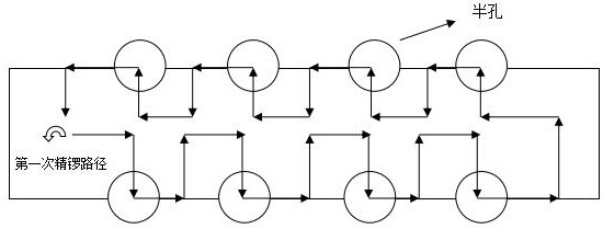
[0072] S300. Carry out the first finishing operation on the circuit b...

Embodiment 2

[0117] As another aspect of the embodiments of the present application, a printed circuit board is provided, which is prepared by the method as described in the first embodiment.

[0118] In summary, the present invention cancels the half-hole process before etching, and completes the half-hole processing in the forming process, and in the process of forming half-holes, the process of forming half-holes is divided into rough and fine, and the fine process is divided into Two times of processing, each fine gong only processes half of the hole wall, avoiding burrs and burrs in the hole when the gong knife cuts the copper layer in the half hole, and avoiding the surface of the printed circuit board before soldering. Hollowing reduces the difficulty of solder mask processing for half-hole plates.


PUM


Abstract

The application provides a half-hole board molding processing method and a printed circuit board. The method includes steps: pretreatment, drilling, copper sinking / board electrical, outer circuit, pattern electroplating, etching, solder mask, text, surface treatment, Forming, the forming steps include one rough gong and two fine gongs. First, the circuit board is slotted through the rough gong; then the circuit board is fixed on the cardboard, and the cardboard is used to support the circuit board; Machining from the side to the right, cutting to half of the hole wall; the second fine gong is processed from the right to the left of the half hole, cutting the remaining part of the hole wall, and the path of the gong cutter for each fine gong is convex and concave. The invention cancels the semi-hole process before etching, and completes the half-hole in the forming process. The process of the half-hole is divided into coarse and two fine holes, so as to avoid burrs and burrs in the half-hole, and the circuit is fixed by the cardboard. The plate supports and protects the gong knife, and at the same time, the cardboard can be replaced automatically to save labor.

Description

technical field [0001] The invention relates to the technical field of printed circuits, in particular to a method for one-time forming of a half-hole plate and a printed circuit board. Background technique [0002] In the field of communication equipment, some printed circuit boards need to be designed as a mother board and a daughter board, which are welded together with the pins of the mother board components through the entire row of semi-metallized holes on the daughter board. Usually, the daughter board generally has a whole row or four sides. Designed as a half hole. The main difficulty in half-hole plate processing is that during the process of gong half-hole, when the rotating ground knife cuts and welds the ring, the copper layer in the hole will produce burrs and burrs, which will affect the use of the half-hole plate. [0003] At present, the main process of making half-hole plate is: adding a half-hole process between pattern electroplating and etching, after p...

Claims


Application Information

Patent Timeline
Patent Type & Authority Patents(China)
IPC IPC(8): H05K3/04H05K1/02
CPCH05K1/02H05K3/04
Inventor 胡志强张仁军邓岚孙洋强牟玉贵李清华
Owner 四川英创力电子科技股份有限公司
Learn More